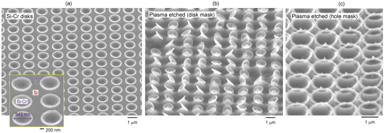
Figure 5.
(a) SEM image of the Si–Cr alloy disk formed on the Cr film (30 nm), imaged after Cr-etch. Pulse energy nJ. (b) SEM images of Si-Cr disks used as dry plasma etch mask followed by Cr-etch. (c) SEM image of Si-Cr rings used as dry plasma etch mask followed by Cr-etch. Laser patterning was carried out with ; diffraction limited focal diameter nm; wavelength nm. Plasma etch was for 5 min.

