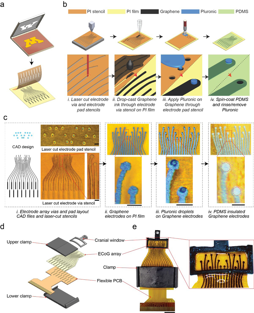
Figure 1 |. Stencil-printed flexible graphene ECoG array:
(a) Stencil-printing adapted from screen-printing to flexible neural interfaces. (b) Schematic of the graphene ECoG electrode array fabrication procedure. (i) Stencils are cut from insulating polyimide tape (PI) using a desktop laser; (ii) After tape-transferring the stencil onto a PI film, graphene ink was drop-cast via stencil on the PI film to pattern the electrode traces, followed by annealing; (iii) After removing the electrode stencil from the PI film, Pluronic sacrificial layer is deposited through the electrode pad stencil on the graphene electrodes; (iv) Once the Pluronic layer solidifies, the electrode pad stencil is carefully removed from the graphene electrode array. Diluted PDMS is spin coated to form the insulating layer. After the PDMS cures, the Pluronic layer is rinsed away to expose the electrode pads. (c) (i) Computer-aided design (CAD) drawing and images of laser-cut stencils for electrode array vias and electrode pads. (ii) The patterned graphene electrode on PI film. (iii) Pluronic droplets on graphene electrodes. (iv) PDMS insulated graphene electrodes. Scale bars indicate 500 μm. (d) CAD rendering of the whole implant assembly. The PDMS-insulated graphene ECoG electrode array is first bonded to a flexible PCB using silver epoxy adhesive to connect the ECoG array with the PCB’s gold pads. The bonded PCB and ECoG array are mechanically reinforced by a 3D printed clamp. (e) Photograph of a fully assembled 16-channel graphene ECoG device. Scale bar indicates 5 mm.

