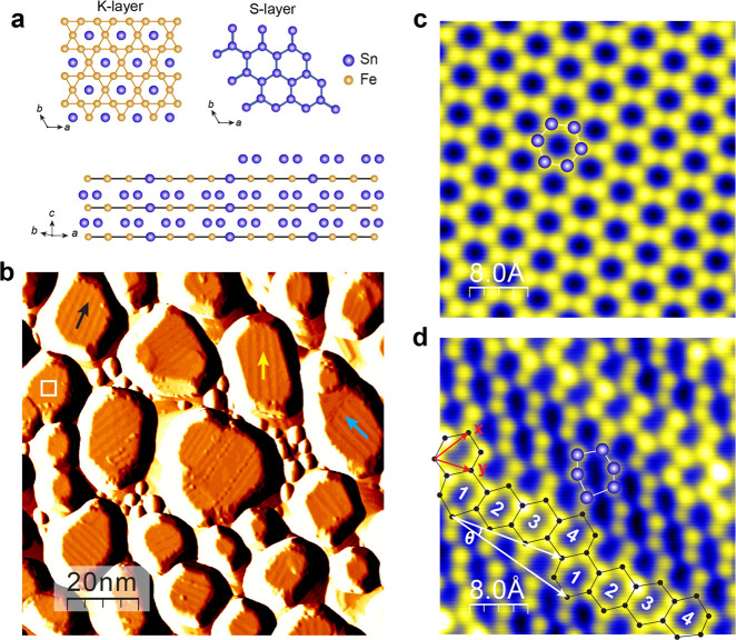
Figure 1.
Molecular beam epitaxy growth of FeSn films on SrTiO3(111). a, Ball-and-stick model of the FeSn crystal structure from top and side views. b, Morphology of a FeSn film grown at Tsub = 480 °C, set point: V = 3.0 V, I = 10 pA. The STM image is in differential mode, and the height of the islands varies from to 6 to 7 nm. c, Atomic resolution STM image showing a perfect honeycomb lattice on the surface of a flat FeSn island, set point: V = −2.0 mV, I = 5.0 nA. d, Atomic resolution image revealing strongly distorted Sn honeycombs on the island with stripe modulations, set point: V = 20 mV, I = 5.0 nA.

