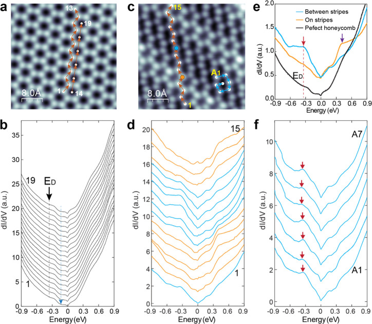
Figure 3.
Modulations of the electronic structure in strained FeSn/SrTiO3(111) films. a, Atomic resolution image of perfect honeycomb lattice, set point: V = 3.0 V, I = 10 pA. b, A series of dI/dV spectra taken at sites marked in (a). The energy position of the Dirac point ED is marked by the black arrow and dashed line, and the dip feature at −0.15 eV is marked by a cyan arrow. c, Atomic resolution image of distorted Sn honeycomb with stripe modulations, set point: V = 10 mV, I = 1.0 nA. d, A series of dI/dV spectra taken at sites marked in (c). The dI/dV spectra are classified into two groups, orange (taken on stripes) and cyan (taken between stripes). e, dI/dV spectra taken at sites on (orange) and between stripes (cyan), compared to the reference spectrum taken on perfect Sn honeycomb without stripe modulations. The pronounced peak at E = −0.36 eV (denoted with red arrow and dashed line) coincides with the Dirac point. f, dI/dV spectra taken within one-unit-cell of the strongly deformed honeycomb lattice, marked in (c). The energy position of the ED is uniform within the deformed honeycomb lattice. The set point remains the same during the line dI/dV measurements.

