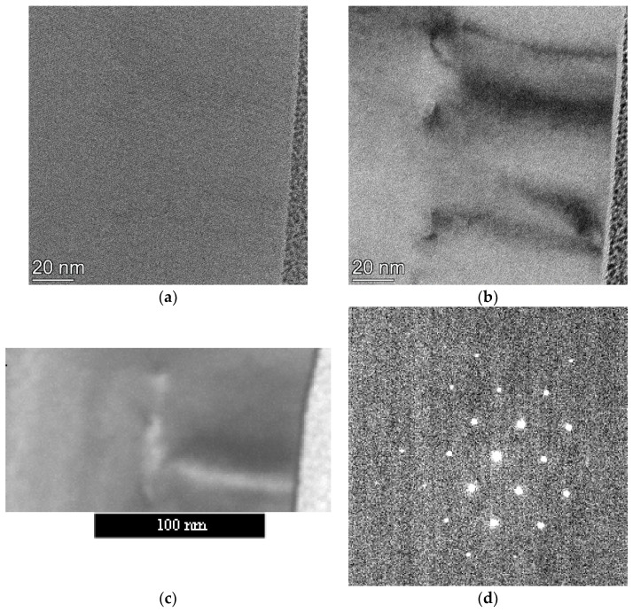
Figure 1.
Example of selecting area and collecting 4D-ED data set: (a) HRTEM image of an area of the sample; (b) BF image of the same area with enhanced contrast around defects; (c) STEM image from the sub-area from where the 4D-ED dataset is collected; (d) Diffraction pattern recorded with the nearly parallel (α = 0.24 mrad) beam from an area of 1 nm diameter (the size of the beam in this mode). A total of 20,000 such patterns form the 4D-ED dataset.

