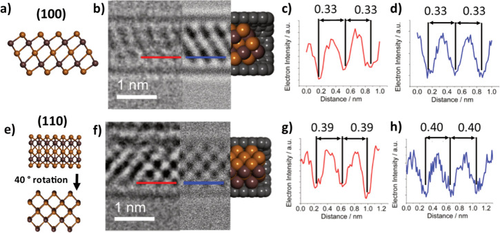
Figure 5.
(a) Structural model of monolayer β-In2Se3 in the (100) orientation. (b) Three-part composite image of an InSe nanoribbon inside a SWCNT, consisting of an AC-TEM image (left), a simulated TEM image (center), and molecular model (right). (c, d) Electron density profile maps in red, generated from the red line superimposed over the experimental AC-TEM image in (b), and in blue, generated from the blue line superimposed over the simulated TEM image in (b), with calculated interatomic distances highlighted in nm. (e–h) The same as (a–d), respectively, but for a different nanoribbon in the (110) orientation.

