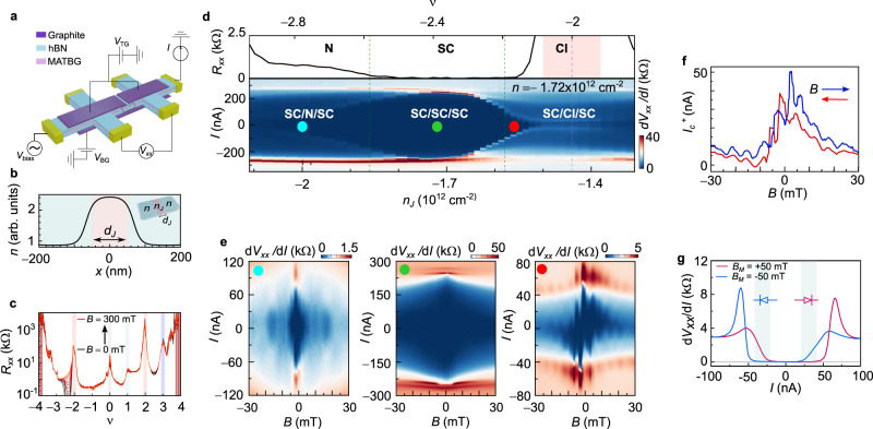
Fig. 1. Gate-tunable JJ in MATBG.
a Schematic of the measured device and measuring circuit, where Vbias is the source voltage, I is the current through the device, Vxx the voltage drop between the measurement probes, and VBG (VTG) correspond to the back (top) gate voltage. The top graphite gates are separated by 150 nm. b Electrostatic simulation profile of carrier density n vs. position x, setting n and carrier density in the junction nJ at different values with a junction length dJ of 100 nm. The inset shows a schematic of the MATBG JJ with two distinct regions created by the gating structure. c Four terminal longitudinal resistance Rxx vs. filling factor υ at different out-of-plane magnetic fields B from 0 mT (black curve) to 300 mT (red curve). d (Top) Magnification of c around the superconducting state −3 < υ < −1.8, where we define three distinct regions with metallic (N), superconducting (SC), and correlated insulator (CI) behavior. (Bottom) vs. I at different nJ, keeping n = −1.72 × 1012 cm−2 in the SC state. Dashed green vertical lines mark the position where nJ is no longer in the SC state. e Fraunhofer patterns measured at (left) nJ = −2 × 1012 cm−2 (SC/N/SC), (center) −1.72 × 1012 cm−2 (SC/SC/SC), and (right) −1.56 × 1012 cm−2 (close to SC/CI/SC), respectively. The color dots show the corresponding nJ positions in the dVxx/dI vs. I map in d bottom. f Positive critical current Ic+ vs. B with B sweeping up (blue) and down (red). g dVxx/dI vs. I at B = 0 mT after applying a pre-magnetizing field BM = + 50 and −50 mT for the red and blue curve. The shaded gray regions mark the values of current at which the diode behavior is observed.

