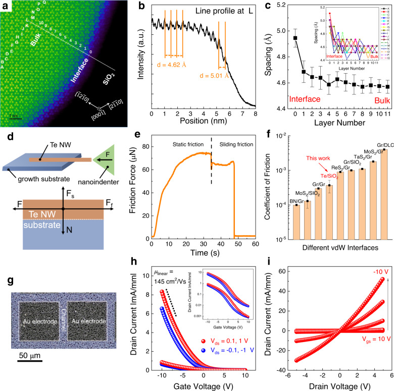
Fig. 3. Multi-scale vdWs integration.
a Cross-sectional high-angle annular dark field scanning transmission electron microscopy (HAADF-STEM) image of Te NW/SiO2. b Line intensity profile located at L position in the HAADF-STEM image. c The average plane spacing of () as a function of layer number ranging from interface to bulk. The measurement was reproduced on 17 samples and the error bar represents the standard deviation. Inset of (c) shows the measurement results of 17 samples. d Schematic illustration of the friction property test. F, Fs, Ff, and N represent the load force, supporting force, friction force, and cohesive force, respectively. e The corresponding friction force measured in the friction property test. The vertical dashed line indicates the boundary between the static friction process and the sliding friction process. f Comparison of the coefficient of friction of various vdWs interfaces. The corresponding references could be found in Supplementary Table 2. g Optical image, h transfer, and i output characteristic curves of the p-type Te nanomesh thin-film transistors (TFTs) fabricated on SiO2. Inset of (h) shows the transfer curve using logarithm y-coordinate.

