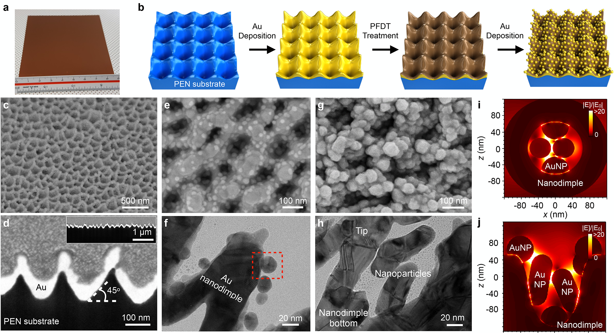
Figure 2. Fabrication and characterization of Au nanoparticle on nanodimples (NPOD) chip.

(a) Photograph of fabricated NPOD chip in 9 cm × 9 cm. The chip can be cut into smaller sizes. (b) The schematic diagram for the fabrication procedure of the NPOD chip. Reactive ion-etching of a polyethylene naphthalate (PEN) substrate and subsequent Au deposition make high-density gold nanodimple structures. The self-assembled monolayer coating of 1H,1H,2H,2H-perfluorodecanethiol (PFDT) and additional Au deposition produce NPOD chips. (c-d) Scanning electron micrographs (SEM) of Au nanodimple structures on top (c) and cross-section (e) views. The inset of (d) shows the cross-section in low magnification to show the uniformity of the high-density nanodimple structures. (e-f) SEM (e) and transmission electron micrograph (TEM, f) of NPOD structures after 10 nm Au deposition on PFDT coating. A zoomed-in image of a red dashed box region is shown in Figure S3. (g-h) Top view of SEM (g) and TEM (h) of NPOD structures after 80 nm Au deposition on PFDT coating. (i-j) 3D finite-difference time-domain (FDTD) simulations of NPOD structures with 80 nm Au deposition in the top (i) and side (j) views, showing plasmonic hotspots between Au nanoparticles as well as Au nanoparticle and nanodimple structures.
