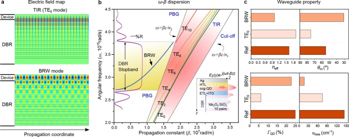
Extended Data Fig. 3. Photonic modelling of the BRW devices developed in the present study.
a, Contour maps of a TE field of the fundamental TIR mode (top) and the BRW mode (bottom) supported by the structure with the transverse DBR-Ag cavity. The optical field of the BRW mode is confined primarily in the device layer (waveguide core), whereas the TIR mode concentrates at the device–DBR interface and leaks into the DBR. b, The calculated ω–β dispersion (ω is the photon angular frequency and β is the modulus of the wavevector) of the TE modes allowed in the BRW structure (depicted in the inset). In this case, the highest (n2) and lowest (n1) index materials of the waveguide are Nb2O5 and SiO2, respectively. There are no waveguided modes for neff (= βc/ω) > n2, which corresponds to the ‘cut-off’ regime. In the range n1 < neff < n2 (red-shaded area), several TIR modes are supported by the waveguide owing to reflections from various layers of the thick DBR stack. The range neff < n1 corresponds to a photonic bandgap or a stopband defined by the reflection spectrum of the DBR (purple line). A BRW mode (blue line) is located in the stopband of the photonic structure. c, A comparison of guided mode parameters between the TE0 TIR (pink) and BRW (orange) modes of the DBR-based structure (Fig. 2b) and the TE0 TIR mode (red) of the reference device (Fig. 2a). The calculated parameters include the effective refractive indices (neff), the modal angles (θm), the mode confinement factors for the ccg-QD layer (ΓQD) and the optical-loss coefficients (αloss).

