
Figure 5.
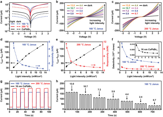
Photoconductors based on Janus NCs. a) I–V characteristics of thin‐film photoconductors made from Janus NCs (synthesized at 160 and 200 °C) and 16 nm CsPbBr3 NCs, under dark (dashed lines) and illumination (450 nm, 13.0 mW cm−2, solid lines). The external bias is 3.0 V. b,c) I–V characteristics under different light intensities (from 0.7 to 13.0 mW cm−2) for devices based on Janus NCs. d–f) Photocurrent, responsivity, and detectivity of devices based on Janus NCs synthesized at 160 and 200 °C, respectively. Inset in (f) shows the detectivity of devices based on 16 nm CsPbBr3 NCs. g) On–off switching behavior of devices operated under the bias of 3.0 V and illumination light intensity of 13.0 mW cm−2. h) On–off switching of devices based on Janus NCs synthesized at 160 °C under varied light intensities.