Figure 3.
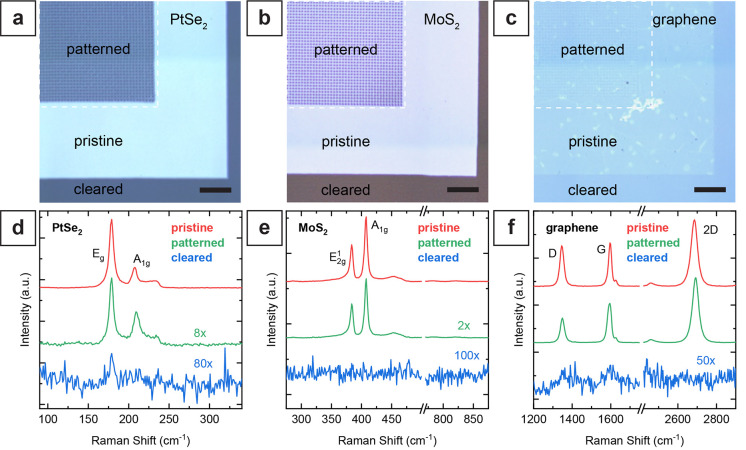
Raman characterization of the patterned 2D materials on glass coverslips. (a–c) Optical microscope images of patterned PtSe2, MoS2, and graphene samples. Raman scans were performed on pristine, patterned, and cleared regions for each material. Scale bars, 10 μm. (d–f) Averaged Raman spectra of pristine (red), patterned (green), and cleared (blue) regions of PtSe2, MoS2, and graphene. The spectra of the patterned areas show the expected modes with reduced intensity due to the material ablation. The mode characteristics of each material show no significant degradation of material quality for the patterned regions. The area where the 2D material was fully removed only shows weak or no corresponding Raman signal (blue line). In (d), (e), and (f), the spectra with low intensity are presented with different scaling factors for better visibility: 8× for patterned PtSe2, 80× for areas cleared from PtSe2, 2× for patterned MoS2, 100× for areas cleared from MoS2, and 50× for areas cleared from graphene.

