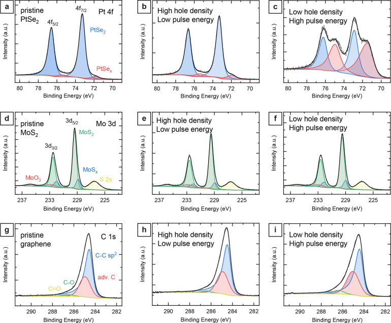
Figure 4.
Comparison between pristine and laser structured 2D materials by X-ray photoelectron spectroscopy (XPS). (a) Characteristic Pt 4f spectrum of pristine PtSe2 with the Pt 4f doublet binding energies at 73.3 eV for 4f7/2 and 76.6 eV for 4f5/2. (b) Pt 4f orbital of PtSe2 film exposed using a high-density nanohole pattern (300 nm hole-to-hole pitch) and using low pulse energy (20 pJ). (c) Pt 4f orbital of PtSe2 film exposed using a low-density nanohole array (1 μm hole-to-hole pitch) and high pulse energy (500 pJ). (d) Characteristic Mo 3d spectrum of the transferred MoS2 film with the Mo 3d doublet binding energies at 229.4 eV for 3d5/2 and 232.5 eV for 3d3/2. (e) Mo 3d orbital of MoS2 film exposed using a high-density nanohole pattern (300 nm hole-to-hole pitch) and using low pulse energy (100 pJ). (f) Mo 3d orbital of MoS2 film exposed using a low-density nanohole array (4 μm hole-to-hole pitch) and high pulse energy (500 pJ). (g) Carbon 1s spectrum of the pristine graphene layer with the asymmetric C–C sp2 band binding energy at 284.5 eV. (h) Carbon 1s orbital of graphene exposed using a high-density nanohole pattern (300 nm hole-to-hole pitch) and using low pulse energy (150 pJ). (i) C 1s orbital of graphene exposed using a low-density nanohole array (4 μm hole-to-hole pitch) and high pulse energy (500 pJ).

