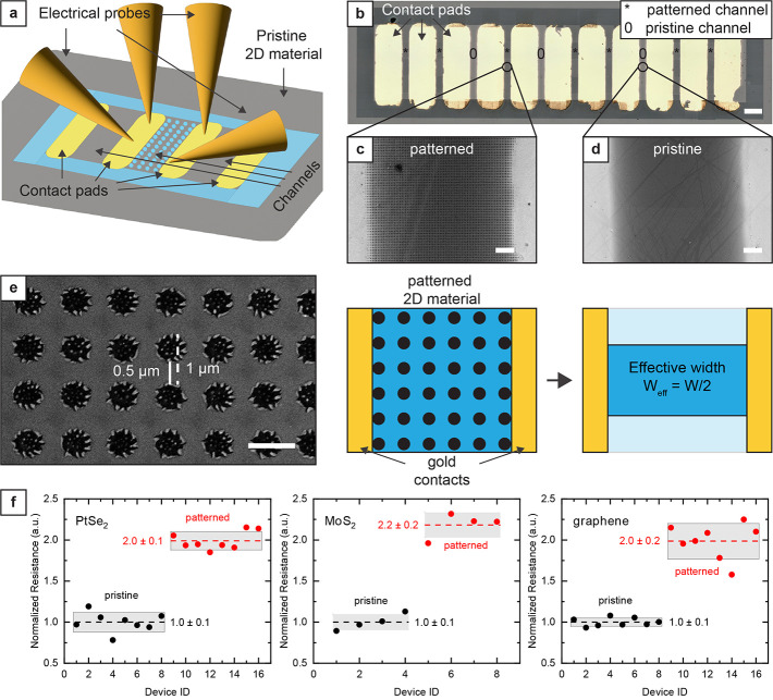
Figure 5.
Electrical characterization of 2D materials patterned by high-speed laser direct writing. (a) Schematic of the device configuration for the electrical characterization of the patterned 2D materials. The 2D material surrounding the electrode array was removed by laser direct writing to electrically isolate the array of devices from the surrounding 2D material layer and define the device channel geometry. Depending on the resistance value, either a two- or four-point probe measurement of the electrical resistance was performed by sweeping either the current or the voltage. (b) Optical microscope image of 10 test structures for electrical characterization of the 2D material channels. Each test structure consists of two gold contact pads and a channel with either a pristine (marked with “0”) or a patterned (marked with “*”) 2D material patch connecting the two electrodes. Scale bar, 200 μm. (c) and (d) are SEM images showing sections of, respectively, patterned and pristine channels between the gold contact pads. Scale bar, 10 μm. (e) SEM image and schematic illustrating the physical constriction of the conductive path due to the patterned nanohole array. Since the hole diameter and pitch are 500 nm and 1 μm, respectively, the effective width of the channel due to the nanohole array is halved. Scale bar, 1 μm. (f) Measured resistances of pristine channels and channels with nanohole array patterns normalized on the average resistance of the pristine channels. The channels consisting of the patterned 2D materials have a significantly higher resistance (2 times higher) than those consisting of a continuous 2D material film due to the constriction of the conductive path.

