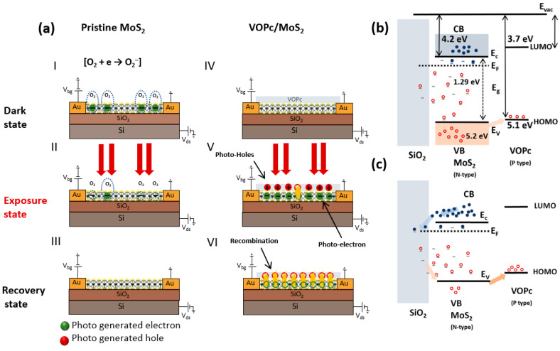
Figure 3.
Photoresponse phenomenon and energy band diagram of micro-phototransistor. (a) Phenomenon of the light at the interface of pristine MoS2 (panels (I, II, III)) and VOPc/MoS2 (panels (IV, V, VI)) heterojunction phototransistor. Panels (I, IV) in dark state, panels (II, V) in exposure state, and panels (III, VI) in recovery state. (b) Energy band diagram of Si substrate, MoS2, and VOPc molecules. (c) Generation of holes by applying the positive gate bias in VOPc/MoS2 heterojunction phototransistor.

