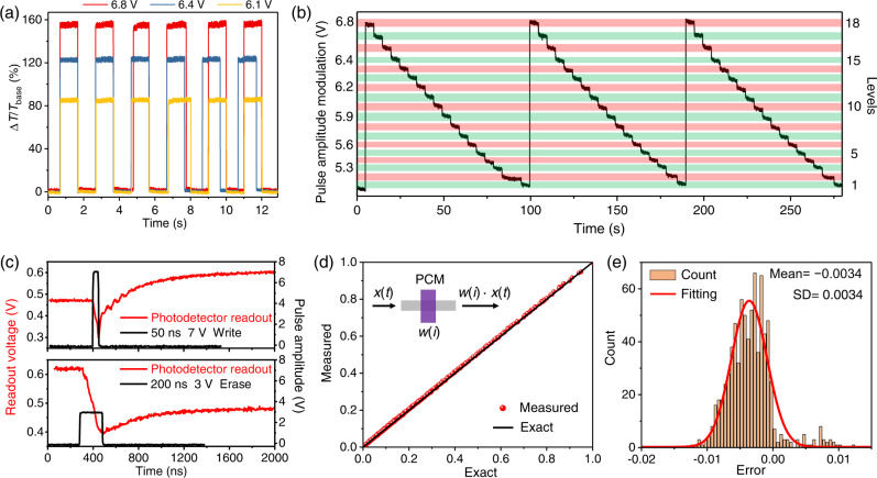
Fig. 2. Electrically reprogrammable photonic waveguide memory cells with over 4-bit encoding levels for scalar multiplication.
a Reversible electrical binary programming of a GST/SiO2 cell (LGST = 2.5 μm, thickness = 30/50 nm and Ldope = 3 μm) by 6.8 V (red), 6.4 V (blue), and 6.1 V (orange) 50-ns Write pulses and fixed 3 V 200-ns Erase pulses. b Multilevel operation of a device showing over 4-bit non-volatile memory levels using pulse amplitude modulation (PAM). c Temporal switching dynamics (red curves) showing amorphization to a higher transmission level achieved with a single 50-ns 7 V rectangular Write pulse (black curve), and recrystallization back to the baseline achieved by a single 200-ns 3 V rectangular Erase pulse (black curve). d Measured scalar multiplication results versus exact results by performing 784 multiplication operations (w(i) × x(t)) mapped by 16 different encoding levels (w(i), i = 1 to 16) of a GST cell as multiplicand (reached with write pulse energy between 5.2 nJ and 8.8 nJ), and 49 random input amplitudes of a probe light (x(t), t = (j − 1)·∆t, ∆t = 1 ms, and j = 1 to 49) as multiplier modulated sequentially by a variable optical attenuator (VOA) at a frequency of 1 kHz. e A histogram of computational error calculated by subtracting the measured scalar multiplication from the exact. The histogram is fitted by a Gaussian distribution (red solid curve). SD standard deviation.

