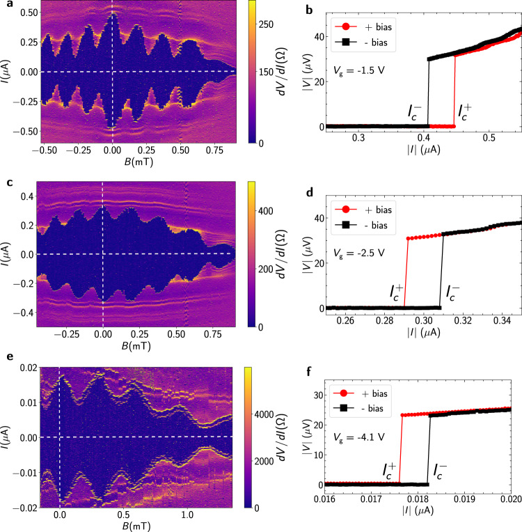
Fig. 4. Polarity reversal of the diode effect.
Differential resistance map of Device 1 as a function of I and B, with all three split gates set to a value of (a) −1.5 V, (c) −2.5 V, and (e) −4.1 V. The crosshairs shown by white dashed lines are at zero values of B and I. I–V characteristics for both bias directions at B = 0.04 mT, with all three split gates set to a value of (b) −1.5 V, (d) −2.5 V, and (f) −4.1 V, showing the reversal of the diode polarity.

