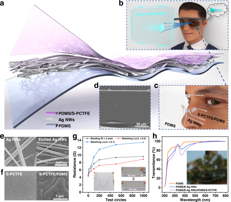
Fig. 1. Schematic illustration of TENG-based electrostatic interface.
a Explosive view of the interface. b Illustration of the interface-based eye-controlled input modality. c The interface array exploded show in front of eye. d SEM image of the layered interface. e SEM images of the raw and etched Ag NWs. f SEM images of the sputtered single layer PCTFE (S-PCTFE) and S-PCTFE grafted on PDMS (S-PCTFE/PDMS). g Surface resistance of bended and stretched Ag NWs electrode on PDMS. (Bending radius at about 3 mm. Data are presented as mean (SD) with error of repeated tests: n = 5). Insert: Digital photos of the bended and stretched electrode. h UV-Vis transmittance spectra of various layers of the interface. Insert: Digital photo of the interface array.

