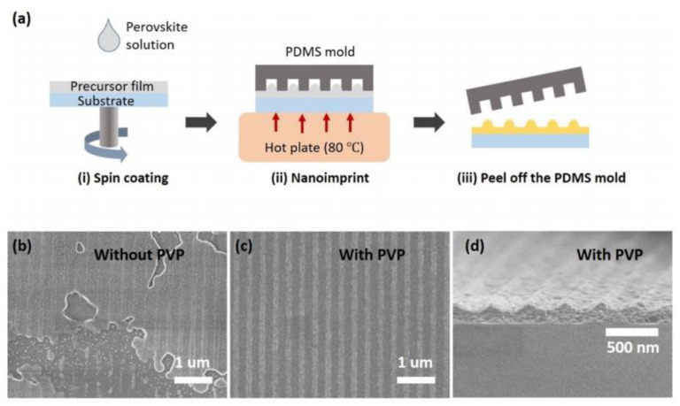
Figure 10.
(a) Scheme of the process for fabricating a perovskite DFB cavity. Top-view SEM images of nanopatterned perovskite films without (b) and with (c) 20% polyvinylpyrrolidone (PVP). (d) Cross-sectional SEM image of the nanopatterned perovskite film with 20% PVP. © American Chemical Society. Copyright 2022 ACS Photonics.

