Figure 2.
Formation of two-dimensional (2D) PET thin films
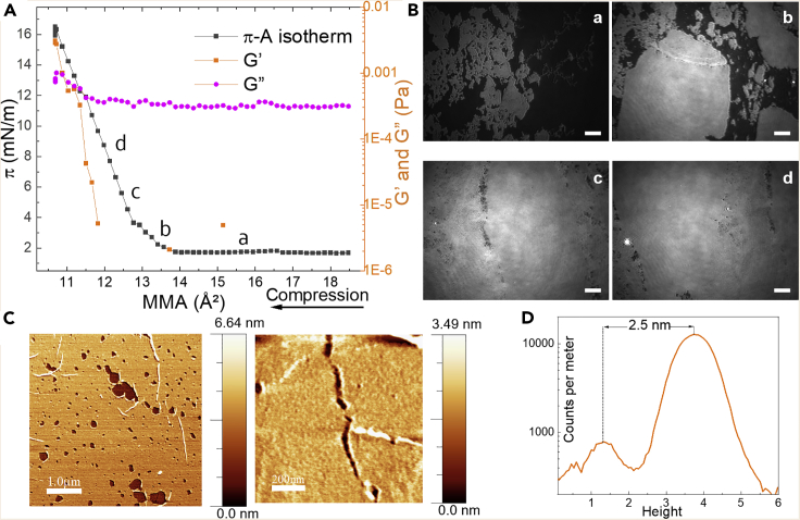
(A) π-A isotherm (black line) and G″ and G′ as a function of mean molecular area (orange and pink lines) measured at the A-W interface.
(B) In situ BAM images taken at given points marked in the isotherm; 50 μm scale bar. See also Figure S1.
(C) AFM images of films transferred to Si wafers at point (c). From left to right: 1 × 5 (1 μm scale bar) and 1 × 1 μm scan (200 nm scale bar).
(D) Height count for AFM images.

