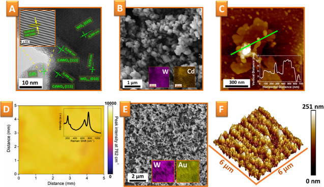
Figure 3.
(A) HRTEM image of WO3/CdWO4/CdS, prepared by annealing at 700 °C of pristine WO3/CdS flakes (the inset reveals the FFT image of CdS); (B) SEM images of WC-700 flakes; (C) AFM scan and surface profile of a single WC-700 flake; (D) Raman mapping of the WC-700 distribution on the Au grating surface; and (E) SEM–EDX and (F) AFM measurements of the Au/WC-700 photoelectrode surface after the deposition of WC-700 flakes on Au grating.

