

Abstract

Cadmium arsenide (Cd3As2) thin films feature a two-dimensional topological insulator (2D TI) phase for certain thicknesses, which theoretically hosts a set of counterpropagating helical edge states that are characteristic of a quantum spin Hall (QSH) insulator. In devices containing electrostatically defined junctions and for magnetic fields below a critical value, chiral edge modes of the quantum Hall effect can coexist with QSH-like edge modes. In this work, we use a quantum point contact (QPC) device to characterize edge modes in the 2D TI phase of Cd3As2 and to understand how they can be controllably transmitted, which is important for use in future quantum interference devices. We investigate equilibration among both types of modes and find non-spin-selective equilibration. We also demonstrate the effect of the magnetic field on suppressing equilibration. We discuss the potential role of QSH-like modes in a transmission pathway that precludes full pinch-off.
Keywords: Topological insulator, quantum point contact, quantum Hall effect, quantum interference, spin−orbit coupling
Quantum point contacts (QPCs) allow for selective and controlled transmission of individual integer and fractional quantum Hall edge modes,1 opening avenues for fundamental physics studies of quantum Hall states and novel device applications. Such applications include electron optical devices, quantum Hall interferometry, and detection of non-Abelian quasi-particle statistics.2−6 To date, only a few investigations of QPCs have focused on topologically nontrivial materials.7 QPCs in two-dimensional topological insulators (2D TIs) would allow for advancing the experimental understanding of their unique edge states and create building blocks for interference experiments that would be useful for future topological quantum information systems. For example, the manipulation of counterpropagating helical edges states with QPCs has been proposed for studies of quantum entanglement, creation and detection of Majorana bound states, and studies of interactions.7−14
Epitaxial cadmium arsenide (Cd3As2) thin films provide a platform for realizing QPCs in a topological material. In particular, recent work has found that thin, (001)-oriented Cd3As2 films possess a nontrivial gap in their two-dimensional electronic states and are thus expected to host helical edge modes characteristic of the quantum spin Hall (QSH) state.15 Similar to graphene,16−20 both electron- and hole-like edge channels can be simultaneously present in electrostatically defined QPCs. Moreover, as schematically shown in Figure 1a, when the Fermi level is in the gap of the 2D TI, a set of counterpropagating, spin-polarized edge modes exists below a critical field (Bc). We denote these edge channels as QSH-like, since they are not topologically protected by time reversal symmetry, in contrast to the helical edge modes at B = 0, and therefore there may be a mini-gap in the edge states.21−23 In a locally gated device, these QSH-like edge states can coexist with chiral edge states of the quantum Hall effect.24 At B = Bc the band order transitions to trivial (uninverted), and for B > Bc there are no edge states when the Fermi level is located in the gap (filling factor ν = 0).
Figure 1.

QPC device and Landau level spectrum. (a) Schematic of Landau levels and edge states of a typical 2D TI in the inverted state at B < Bc (9 T) and in the trivial (uninverted) regime (14 T). Gray areas mark the energy ranges where heavy hole states do not allow for higher-order hole-like Landau levels to be resolved (left region in the experimental Landau level spectrum shown in Figure 1d). (b) QPC device schematic and contact configurations. (c) Scanning electron micrograph of representative QPC split gates from a different chip fabricated using the same parameters. (d) Landau level spectrum showing longitudinal conductivity as a function of magnetic field B and gate voltage Vg, measured on a Hall bar device. The filling factor ν is assigned based on the quantum Hall plateaus shown in Figure S2.
In this work, we report on a QPC device fabricated on a Cd3As2 thin film. We demonstrate individual transmission and pinch-off of quantum Hall edge modes in quantizing magnetic fields. We show that full pinch-off is avoided in the inverted regime below Bc, which may be attributed to the QSH-like modes providing a pathway for transmission when the split gates or constriction are tuned into the topological gap. When electron-like edge modes accumulate under the split gates, we observe equilibration from mixing between modes. This mixing is suppressed by sufficiently strong magnetic fields and is less efficient at higher ν. When a hole-like edge mode is localized under the split gates, we observe equilibration with reflected electron-like modes. We find that in both cases, this equilibration is not spin-selective, in contrast to other systems.
Figure 1b shows a schematic top view of the device. Electron beam lithography (EBL) was used to pattern 10 μm Hall bar mesas from a 20-nm-thick Cd3As2 film grown by molecular beam epitaxy, as described elsewhere.25 Mesa isolation was performed by using argon ion milling. The etched areas were filled in with an SiO2 field dielectric to isolate the following layers from the substrate. Ohmic Ti–Pt–Au contacts to the mesa arms were deposited via electron beam evaporation. A blanket Al2O3 gate dielectric was deposited via a 120 °C atomic layer deposition (ALD) process. The QPC split gates were patterned using EBL, followed by thermal evaporation of a 5/30 nm Ni/Au stack. Figure 1c shows that the QPC split gate separation is 120 nm. Larger gate contacts were patterned with photolithography and metallized with electron beam evaporation (Ti/Pt/Au) to make contact with the split gates. A second ALD Al2O3 gate dielectric was deposited and selectively removed from the ohmic and gate pads using an inductively coupled plasma etch. Lastly, a global top gate (5/30 nm Ni/Au) was patterned with photolithography and metallized with thermal evaporation (see Figure S1 for a micrograph of the device). All magnetotransport measurements were taken at 2 K by using a He-4 cryostat. An alternating current of 1.35 nA at 17.777 Hz was sourced, and lock-in amplifiers were used to measure voltages.
The three voltages measured are Hall (VH), diagonal (VD), and longitudinal
(VL) voltages, respectively (Figure 1b). For each, the
conductance
is defined as G = I/V, where I is the constant source current. The voltage
applied to the split gates (VQPC) electrostatically
defines the constriction and also controls the filling factor, νg, under the split gates, which can be estimated from the capacitance
of the top gate. The voltage applied to the global top gate (VTG) determines the filling factor in the bulk
of the device (νb) and hence the number of edge modes
flowing into the QPC, as indicated by the Hall conductance 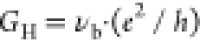 . The global top gate is screened by the
underlying split gates and has no effect on the region under the split
gates or on νg. The (average) filling factor in the
constriction (νQPC) is modulated by both the split
and top gates. The diagonal conductance GD reflects the number of edge modes transmitted through the constriction
and is discussed below.
. The global top gate is screened by the
underlying split gates and has no effect on the region under the split
gates or on νg. The (average) filling factor in the
constriction (νQPC) is modulated by both the split
and top gates. The diagonal conductance GD reflects the number of edge modes transmitted through the constriction
and is discussed below.
A Landau level spectrum, obtained by measuring the longitudinal and Hall resistances on a gated Hall bar from the same Cd3As2 film and converting them into the longitudinal conductivity (σxx), provides the landscape of filling factors probed by the QPC as a function of the magnetic field and global top gate voltage (Figure 1d). All degeneracies are lifted, giving rise to even and odd integer quantum Hall plateaus (see Figure S2). The zero-energy Landau levels cross at Bc ≈ 9.5 T, marking the transition between topologically nontrivial and trivial regimes (see ref (15) for a detailed discussion). In the following, we discuss the performance of the QPC in detail at two different fields: just below the phase transition (B = 9 T) and above it (B = 14 T). We first discuss results in the accumulation regime (νg > νb), followed by a discussion of transmission (νg = νb), pinch-off (νg < νb), and inversion (νg ≤ 0).
Accumulation Regime
We begin by studying the QPCs at
9 T. In Figure 2a, VTG is held constant, tuning the bulk to νb = 3 (GH = 3e2/h), while VQPC is modulated. In the accumulation regime (purple
highlighted region), VQPC is tuned such
that νg > νb and additional electron-like modes form under the
split gates,
as schematically shown in Figure 2b. These localized modes can short-circuit the constriction
for 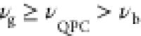 and equilibrate opposite edges of the device,
decreasing the conductance. This equilibration gives rise to the series
of steps in GD seen in Figure 2a as νg changes.
This scenario is similar to an n-n′-n junction, for which the conductance is
given by17
and equilibrate opposite edges of the device,
decreasing the conductance. This equilibration gives rise to the series
of steps in GD seen in Figure 2a as νg changes.
This scenario is similar to an n-n′-n junction, for which the conductance is
given by17
| 1 |
where σ denotes the spin polarization of the associated Landau level and (Nbσ,NQPC) give the number of equilibrating edge modes. A complete set of values of GD calculated from eq 1 for νb = 3 to νb = 1 are shown in Table S1. For νb = 3 at 9 T (Figure 2a), GD exhibits steps at νg = 4 and νg= 5, indicative of equilibration between the three channels from the bulk with the additional channels under the split gates (see, e.g., Figure 2b for νg = 4). The calculated values for GD3,4=12/5 and GD=15/7 are marked in Figure 2a for these steps, which are far below the actual values. A series of steps also occurs in the accumulation regime for νb = 2 (Figure 3a, purple highlighted region) when νg > 2. The values of these steps are also higher than the calculated values.
Figure 2.

QPC operation at 9 T for νb = 3. (a) Line traces of GH (turquoise) and GD (orange) as a function of VQPC. The top gate voltage VTG is set to a value such that νb = 3. Calculated values of the plateaus are shown (see text). The overlay colors indicate the following regimes: accumulation (purple), transmission (aqua), pinch-off (green), and inversion (red). (b–e) Schematics of the edge mode transport for various configurations in the QPC device. Blue modes are electron-like and red modes are hole-like. The yellow highlighted regions indicate equilibration due to edge mode mixing.
Figure 3.

QPC operation at 9 T for νb = 2 and νb = 1. (a) Line traces of GH (turquoise) and GD (orange) as a function of VQPC for νb = 2. (b–e) Schematics of edge mode transport for νb = 2. (f) Line traces of GH (turquoise) and GD (orange) as a function of VQPC for νb = 1. (h–j) Schematics of edge mode transport for νb = 1. The overlay colors indicate the following regimes: accumulation (purple), transmission (aqua), pinch-off (green), and inversion (red). The yellow highlighted regions indicate equilibration due to edge mode mixing.
The results for νb = 3 and νb = 2 thus suggest an incomplete degree of equilibration between the edge modes, which may be explained through a picture of the quantum Hall effect where the edge modes correspond to conducting, compressible strips separated by insulating, incompressible strips.26 In this model, mixing between edge modes involves tunneling through the incompressible strips. Therefore, we expect mixing to be less efficient for higher-order edge modes, because charge must tunnel through multiple incompressible strips.27,28 This picture is confirmed by what is seen for νb = 1 (Figure 3f), where a sharp drop in the conductance from e2/h to ∼0.7e2/h closely matches the expected value of GD1,2 = (2/3)e2/h. Equilibration is thus much more complete for νb = 1, owing to the fewer incompressible strips. Furthermore, this result demonstrates that mixing between electron-like channels is not spin-selective, since the two edge modes involved have opposite spin polarizations.
In contrast to the data at 9 T, there are no signs of equilibration under accumulation at 14 T (Figure 4), as GD remains constant for both νb = 2 (Figure 4a) and νb = 1 (Figure 4f). This suggests that mixing among the electron-like edge states is reduced at 14 T. In the model discussed previously, higher magnetic fields increase the width of the incompressible strips, making tunneling between all edge modes less efficient.26 Evidently, at 14 T the strips are wide enough to completely quench mixing.
Figure 4.

QPC operation at 14 T for νb = 2 and νb = 1 (a) Line traces of GH (turquoise) and GD (orange) as a function of VQPC for νb = 2. (b–e) Schematics of edge mode transport for νb = 2. (f) Line traces of GH (turquoise) and GD (orange) as a function of VQPC for νb = 1. (h–j) corresponding schematics of edge mode transport. The overlay colors indicate the following regimes: accumulation (purple), transmission (aqua), pinch-off (green), and inversion (red). The yellow highlighted regions indicate equilibration due to edge mode mixing.
Transmission and Pinch-Off Regimes
As VQPC is decreased, the device transitions from accumulation
to transmission where  . For νb = νg = 3 (the aqua region in Figure 2a), GD plateaus
at nearly 3e2/h. This
plateau indicates transmission of the three edge modes underneath
the split gates, as schematically shown in Figure 2c. The degree of quantization is poor, likely
due to residual bulk transport at higher filling factors. Accordingly,
quantization is much better at νb = νg = 2 and
. For νb = νg = 3 (the aqua region in Figure 2a), GD plateaus
at nearly 3e2/h. This
plateau indicates transmission of the three edge modes underneath
the split gates, as schematically shown in Figure 2c. The degree of quantization is poor, likely
due to residual bulk transport at higher filling factors. Accordingly,
quantization is much better at νb = νg = 2 and  , see Figure 3a and f.
Upon decreasing VQPC further to νg < νb, pinch-off is expected. For νb = 3 (green region in Figure 2a), the pinch-off of one edge channel is seen, which results in a sharp decrease to a plateau at GD = 2e2/h. This plateau occurs for νg = 1, meaning that the outermost edge mode passes under the split gates, while the other edge mode passes through the constriction, as illustrated in Figure 2d. A similar situation occurs for νb = 2 (Figure 3a), where GD drops from 2e2/h to e2/h. At νb = 1 (Figure 3f), however, there is no pinch-off at any value of νg, even when νg reaches −1. A possible reason is illustrated in Figure 3j and will be discussed below. In contrast, for νb = 1 at 14 T (Figure 4f), full transmission occurs at νg = 1, followed by a gradual decrease in GD for νg ≤ 0 that indicates partial pinch-off, in contrast to the 9 T data.
Inversion Regime
In the inversion regime (νg ≤ 0, red highlighted regions in Figures 2–4), a hole-like mode forms under the split gates, which can mix with incoming electron-like modes, causing equilibration. In this regime, only mixing with reflected electron-like modes has an effect on GD, contributing a fraction of e2/h, whereas transmitted modes will contribute a full e2/h. For example, for νb = 3 (Figure 2a), the increase of GD for νg = −1 corresponds to equilibration between the back-reflected channel and the localized hole-like channel, as illustrated in Figure 2e. Notably, this mixing indicates a lack of spin-selectivity, as the equilibrating channels have opposite spin polarization, which is a departure from findings in other material systems.20,27,28 In general, spin-flip transitions may be facilitated by spin-orbit interaction,24,29−31 which is strong in Cd3As2.32,33 For this scenario, the expected quantitative values of GD under inversion for our device geometry have been determined in prior work20 to be
| 2 |
where σ denotes the spin polarization of the associated Landau level and (Nbσ, Ng, NQPCσ) give the number of equilibrating edge modes. The expected values of GD calculated from eq 2 are shown in Table S2 for both spin-selective and non-spin-selective mixing. For νb = 3 and νg = −1 (Figure 2a) non-spin-selective equilibration occurs between the back-reflected channel and the localized hole-like channel, as shown in Figure 2e. Such a scenario results in GD = (1/2)e2/h from mixing plus an additional GD2,0,2 = 2e2/h from the two transmitted modes, giving a total GD = (5/2)e2/h. Notably, the actual value of GD is significantly less than the calculated (5/2)e2/h, which may again be attributed to limited tunneling through multiple incompressible strips, similar to what is seen in the accumulation regime at 9 T. Equilibration is more complete for νb = 2 (Figure 3a), where GD is closer to the theoretical value of GD = GD1,–1,0 + GD = 1/2 + 1 = (3/2)e2/h.
In contrast to the previous cases, no signs of pinch-off are observed under inversion for νb = 1 (Figure 3f). A possible scenario that would explain why one edge channel is always transmitted for νb = 1 is that the constriction remains at νQPC = 1. An alternative explanation invokes an edge mode picture that is unique to a topological insulator. When νg = 0 and B < Bc, QSH-like edge modes should form under the split gates. As illustrated in Figure 3i, the QSH-like electron mode can connect with the mode from the bulk, allowing for transmission under the split gate. As the split gates are further reduced to νg = −1, the constriction changes to νQPC = 0, and again the electron-like QSH edge mode allows transmission of the mode from the bulk (see Figure 3j). The crossing of the electron- and hole-like QSH modes as shown in Figure 3j occurs to satisfy the differences in filling factors between these various regions and the fact that edge modes cannot terminate. This crossing is facilitated by the very close spatial proximity of the two edge modes. At 9 T, the bands are nearly uninverted, and the momenta of the edge modes within the remnant nontrivial gap are approximately equal (see Figure 1a). Therefore, the modes should nearly coincide along any boundary and permit crossing. Additional compelling evidence for an interpretation that involves the QSH-like modes for the behavior at 9 T can be obtained from a comparison with the 14 T data. At 14 T, no QSH-like modes exist for νg = 0 due to the uninverted band structure. Accordingly, for νb = 1 at 14 T (Figure 4f), the onset of pinch-off of the edge mode by the QPC is seen for νg ≤ 0 by the fact that GD falls below e2/h, unlike what is seen at 9 T. This situation is schematically shown in Figure 4j. Comparison of Figure 3j and Figure 4j illustrates how, for νQPC = 0, the differences in the topological states may become evident in inversion.
To briefly summarize, we studied the operation of a QPC fabricated on a (001)-oriented 2D TI Cd3As2 thin film. We demonstrated the pinch-off of integer quantum Hall edge modes. We found that full pinch-off is avoided when the device is in the inverted (topological) regime, which may be facilitated by QSH-like edge modes providing a pathway for transmission. Equilibration between edge modes is suppressed for higher filling factors and by a magnetic field, owing to the reduced tunneling probability across multiple incompressible strips that widen with increasing field. We observe non-spin-selective equilibration among hole-like and electron-like channels, likely due to the effects of spin-orbit coupling. Future work on these QPCs will focus on an improved understanding of the helical edge modes in the quantum spin Hall state at zero field, which may be achieved in QPCs with etch-defined constrictions.7 Furthermore, a clearer understanding of equilibration and coupling between QH and QSH-like edge modes is needed, which may be achieved in a bipolar junction device with local gating. Both of these elements are essential for optimizing future quantum point contacts and interference devices in 2DTIs.
Acknowledgments
The research was supported by the Office of Naval Research (Grant No. N00014-21-1-2474). Partial support for experiments by S.M. was provided by the CATS Energy Frontier Research Center, which is funded by the Department of Energy, Basic Energy Sciences, under contract DE-AC02-07CH11358. A. R. acknowledges partial support by a grant from the Army Research Office (W911NF-22-1-0016). S. M. and A.C.L. thank the Graduate Research Fellowship Program of the U.S. National Science Foundation for support (Grant Nos. 2139319 and 1650114). R. K. acknowledges support through an appointment to the Intelligence Community Postdoctoral Research Fellowship Program at the University of California, Santa Barbara, administered by Oak Ridge Institute for Science and Education through an interagency agreement between the U.S. Department of Energy and the Office of the Director of National Intelligence. This work made use of the MRL Shared Experimental Facilities, which are supported by the MRSEC Program of the U.S. National Science Foundation under Award No. DMR 1720256.
Data Availability Statement
The data that support the findings of this study are available in the article and its Supporting Information. Raw data can be obtained from the corresponding authors upon request.
Supporting Information Available
The Supporting Information is available free of charge at https://pubs.acs.org/doi/10.1021/acs.nanolett.3c01263.
Micrograph of the device, Hall conductivity data from a Hall bar device, calculated diagonal conductances, complete set of diagonal, Hall and longitudinal conductances at 9 T from the QPC device as a function of VTG and VQPC (PDF)
Author Contributions
S. M. and A. R. designed the device and developed the cleanroom fabrication techniques. S. M. fabricated the QPC devices, performed all QPC measurements, and analyzed the data. A. C. L. grew the film and carried out the Hall bar measurements. R. K. assisted with data collection. S. M. and S. S. prepared the manuscript and all authors commented on it.
The authors declare no competing financial interest.
Due to a production error, there was extra text in the abstract. This was corrected in the version published on June 15, 2023.
Supplementary Material
References
- van Houten H.; Beenakker C.W.J.; van Wees B.J. v. Quantum Point Contacts. Semiconductors and Semimetals 1992, 35, 9–112. 10.1016/S0080-8784(08)62392-3. [DOI] [Google Scholar]
- de C. Chamon C.; Freed D. E.; Kivelson S. A.; Sondhi S. L.; Wen X. G. Two point-contact interferometer for quantum Hall systems. Phys. Rev. B 1997, 55, 2331. 10.1103/PhysRevB.55.2331. [DOI] [Google Scholar]
- Nakamura J.; Liang S.; Gardner G. C.; Manfra M. J. Direct observation of anyonic braiding statistics. Nat. Phys. 2020, 16, 931–936. 10.1038/s41567-020-1019-1. [DOI] [PMC free article] [PubMed] [Google Scholar]
- Bid A.; Ofek N.; Inoue H.; Heiblum M.; Kane C. L.; Umansky V.; Mahalu D. Observation of neutral modes in the fractional quantum Hall regime. Nature 2010, 466, 585–590. 10.1038/nature09277. [DOI] [PubMed] [Google Scholar]
- Bocquillon E.; Freulon V.; Parmentier F. D.; Berroir J.-M.; Placais B.; Wahl C.; Rech J.; Jonckheere T.; Martin T.; Grenier C.; Ferraro D.; Degiovanni P.; Feve G. Electron quantum optics in ballistic chiral conductors. Ann. Phys. 2014, 526, 1–30. 10.1002/andp.201300181. [DOI] [Google Scholar]
- Ji Y.; Chung Y. C.; Sprinzak D.; Heiblum M.; Mahalu D.; Shtrikman H. An electronic Mach-Zehnder interferometer. Nature 2003, 422, 415–418. 10.1038/nature01503. [DOI] [PubMed] [Google Scholar]
- Strunz J.; Wiedenmann J.; Fleckenstein C.; Lunczer L.; Beugeling W.; Muller V. L.; Shekhar P.; Ziani N. T.; Shamim S.; Kleinlein J.; Buhmann H.; Trauzettel B.; Molenkamp L. W. Interacting topological edge channels. Nat. Phys. 2020, 16, 83. 10.1038/s41567-019-0692-4. [DOI] [Google Scholar]
- Teo J. C. Y.; Kane C. L. Critical behavior of a point contact in a quantum spin Hall insulator. Phys. Rev. B 2009, 79, 235321. 10.1103/PhysRevB.79.235321. [DOI] [Google Scholar]
- Dolcini F. Full electrical control of charge and spin conductance through interferometry of edge states in topological insulators. Phys. Rev. B 2011, 83, 165304. 10.1103/PhysRevB.83.165304. [DOI] [Google Scholar]
- Strom A.; Johannesson H. Tunneling between Edge States in a Quantum Spin Hall System. Phys. Rev. Lett. 2009, 102, 096806. 10.1103/PhysRevLett.102.096806. [DOI] [PubMed] [Google Scholar]
- Li J.; Pan W.; Bernevig B. A.; Lutchyn R. M. Detection of Majorana Kramers Pairs Using a Quantum Point Contact. Phys. Rev. Lett. 2016, 117, 046804. 10.1103/PhysRevLett.117.046804. [DOI] [PubMed] [Google Scholar]
- Klinovaja J.; Loss D. Fractional charge and spin states in topological insulator constrictions. Phys. Rev. B 2015, 92, 121410(R) 10.1103/PhysRevB.92.121410. [DOI] [Google Scholar]
- Inhofer A.; Bercioux D. Proposal for an on-demand source of polarized electrons into the edges of a topological insulator. Phys. Rev. B 2013, 88, 235412. 10.1103/PhysRevB.88.235412. [DOI] [Google Scholar]
- Chen W.; Shen R.; Sheng L.; Wang B. G.; Xing D. Y. Electron Entanglement Detected by Quantum Spin Hall Systems. Phys. Rev. Lett. 2012, 109, 036802. 10.1103/PhysRevLett.109.036802. [DOI] [PubMed] [Google Scholar]
- Lygo A. C.; Guo B.; Rashidi A.; Huang V.; Cuadros-Romero P.; Stemmer S. Two-dimensional topological insulator state in cadmium arsenide thin films. Phys. Rev. Lett. 2023, 130, 046201. 10.1103/PhysRevLett.130.046201. [DOI] [PubMed] [Google Scholar]
- Nakaharai S.; Williams J. R.; Marcus C. M. Gate-Defined Graphene Quantum Point Contact in the Quantum Hall Regime. Phys. Rev. Lett. 2011, 107, 036602. 10.1103/PhysRevLett.107.036602. [DOI] [PubMed] [Google Scholar]
- Zimmermann K.; Jordan A.; Gay F.; Watanabe K.; Taniguchi T.; Han Z.; Bouchiat V.; Sellier H.; Sacepe B. Tunable transmission of quantum Hall edge channels with full degeneracy lifting in split-gated graphene devices. Nat. Commun. 2017, 8, 14983. 10.1038/ncomms14983. [DOI] [PMC free article] [PubMed] [Google Scholar]
- Ronen Y.; Werkmeister T.; Najafabadi D. H.; Pierce A. T.; Anderson L. E.; Shin Y. J.; Lee S. Y.; Lee Y. H.; Johnson B.; Watanabe K.; Taniguchi T.; Yacoby A.; Kim P. Aharonov-Bohm effect in graphene-based Fabry-Perot quantum Hall interferometers. Nat. Nanotechnol. 2021, 16, 563–569. 10.1038/s41565-021-00861-z. [DOI] [PubMed] [Google Scholar]
- Abanin D. A.; Levitov L. S. Quantized transport in graphene p–n junctions in a magnetic field. Science 2007, 317, 641–643. 10.1126/science.1144672. [DOI] [PubMed] [Google Scholar]
- Amet F.; Williams J. R.; Watanabe K.; Taniguchi T.; Goldhaber-Gordon D. Selective Equilibration of Spin-Polarized Quantum Hall Edge States in Graphene. Phys. Rev. Lett. 2014, 112, 196601. 10.1103/PhysRevLett.112.196601. [DOI] [PubMed] [Google Scholar]
- Konig M.; Wiedmann S.; Brune C.; Roth A.; Buhmann H.; Molenkamp L. W.; Qi X. L.; Zhang S. C. Quantum spin hall insulator state in HgTe quantum wells. Science 2007, 318, 766–770. 10.1126/science.1148047. [DOI] [PubMed] [Google Scholar]
- Scharf B.; Matos-Abiague A.; Fabian J. Magnetic properties of HgTe quantum wells. Phys. Rev. B 2012, 86, 075418. 10.1103/PhysRevB.86.075418. [DOI] [Google Scholar]
- Zhang S. B.; Lu H. Z.; Shen S. Q. Edge states and integer quantum Hall effect in topological insulator thin films. Sci. Rep. 2015, 5, 13277. 10.1038/srep13277. [DOI] [PMC free article] [PubMed] [Google Scholar]
- Calvo M. R.; de Juan F.; Ilan R.; Fox E. J.; Bestwick A. J.; Muhlbauer M.; Wang J.; Ames C.; Leubner P.; Brune C.; Zhang S. C.; Buhmann H.; Molenkamp L. W.; Goldhaber-Gordon D. Interplay of Chiral and Helical States in a Quantum Spin Hall Insulator Lateral Junction. Phys. Rev. Lett. 2017, 119, 226401. 10.1103/PhysRevLett.119.226401. [DOI] [PubMed] [Google Scholar]
- Goyal M.; Salmani-Rezaie S.; Pardue T. N.; Guo B. H.; Kealhofer D. A.; Stemmer S. Carrier mobilities of (001) cadmium arsenide films. APL Mater. 2020, 8, 051106. 10.1063/5.0002771. [DOI] [Google Scholar]
- Chklovskii D. B.; Shklovskii B. I.; Glazman L. I. Electrostatics of Edge Channels. Phys. Rev. B 1992, 46, 4026–4034. 10.1103/PhysRevB.46.4026. [DOI] [PubMed] [Google Scholar]
- Alphenaar B. W.; McEuen P. L.; Wheeler R. G.; Sacks R. N. Selective Equilibration Among the Current-carrying States in the Quantum Hall Regime. Phys. Rev. Lett. 1990, 64, 677–680. 10.1103/PhysRevLett.64.677. [DOI] [PubMed] [Google Scholar]
- Nicoll G.; Adam C.; Roosli M. P.; Marki P.; Scharnetzky J.; Reichl C.; Wegscheider W.; Ihn T. M.; Ensslin K. Spin-Selective Equilibration among Integer Quantum Hall Edge Channels. Phys. Rev. Lett. 2022, 128, 056802. 10.1103/PhysRevLett.128.056802. [DOI] [PubMed] [Google Scholar]
- Khaetskii A. V. Transitions Between Spin-Split Edge Channels in the Quantum-Hall-Effect Regime. Phys. Rev. B 1992, 45, 13777–13780. 10.1103/PhysRevB.45.13777. [DOI] [PubMed] [Google Scholar]
- Muller G.; Weiss D.; Khaetskii A. V.; Vonklitzing K.; Koch S.; Nickel H.; Schlapp W.; Losch R. Equilibration Length of Electrons in Spin-Polarized Edge Channels. Phys. Rev. B 1992, 45, 3932–3935. 10.1103/PhysRevB.45.3932. [DOI] [PubMed] [Google Scholar]
- Gusev G. M.; Levin A. D.; Kvon Z. D.; Mikhailov N. N.; Dvoretsky S. A. Quantum Hall Effect in n-p-n and n-2D Topological Insulator-n Junctions. Phys. Rev. Lett. 2013, 110, 076805. 10.1103/PhysRevLett.110.076805. [DOI] [PubMed] [Google Scholar]
- Blom F. A. P.; Cremers J. W.; Neve J. J.; Gelten M. J. Anisotropy of the Electronic g*-Factor in Cadmium Arsenide. Solid State Commun. 1980, 33, 69–73. 10.1016/0038-1098(80)90698-5. [DOI] [Google Scholar]
- Bodnar J.Band structure of Cd3As2from Shubnikov-de Haas and de Haas-van Alphen effects, 3rd International Conference on Physics of Narrow-Gap Semiconductors; arXiv:1709.05845; Warsaw, 1978; p 311. [Google Scholar]
Associated Data
This section collects any data citations, data availability statements, or supplementary materials included in this article.
Supplementary Materials
Data Availability Statement
The data that support the findings of this study are available in the article and its Supporting Information. Raw data can be obtained from the corresponding authors upon request.