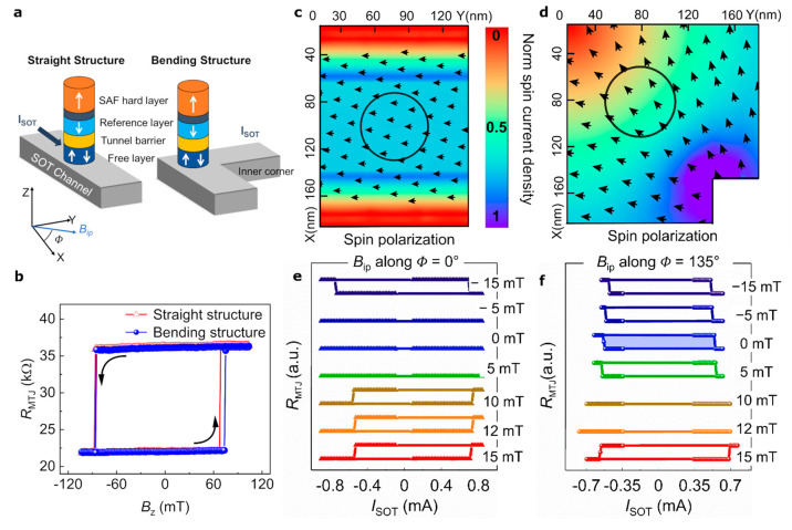
Figure 1.
FFS in bending structure and comparison with straight structure. (a) Schematic showing placement of a pMTJ on the SOT channel for straight and bending structures. (b) Hysteresis loop of the free layer in straight and bending structures. (c, d) Simulated color map of the normalized spin current density (JS) in the SOT channel with the arrows indicating the direction of the spin polarization (σ). (c) The straight structure shows σ pointing along y, and a uniform JS around the MTJ with variations near the edges due to the proximity to VIA contacts. (d) The MTJ in the bending structure experiences a JS gradient and change in the direction of σ due to current bending at the corners. (e, f) Average of 20 DC switching loops for the varied magnitude of Bip along (e) Φ = 0° for the straight structure and (f) Φ = 135° for the bending structure.

