Figure 4.
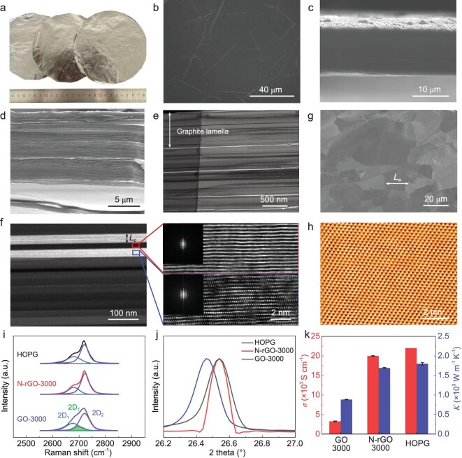
Structure and properties of large-area HOPG-like graphene films. (a) A photograph of three pieces of 10-μm-thick free-standing N-rGO-derived graphene films with a diameter of ∼14 cm. (b–d) SEM images of the surface (b) and cross section (c and d) of the films in (a). The cross-sectional samples in (c) and (d) were fabricated by ion beam cutting and tension fracture, respectively. (e) Cross-sectional BF-TEM image, where the parallel white lines are carbon-deficient interfaces of adjacent graphite lamellae (Supplementary Fig. 14). (f) Cross-sectional ADF-STEM image, in which the parallel bands of different brightnesses are single-crystal graphite grains with different orientations, as proven by HRTEM images and the corresponding Fourier transforms (insets). (g) SEM-ECC image of the film surface. (h) Atomically resolved in-plane STM image, showing a perfect graphite lattice. (i–k) Comparisons of Raman 2D peak (h), (002) XRD peak (i) and electrical and thermal conductivities (j) of GO- and N-rGO-derived graphene films and HOPG.

