
Figure 16.
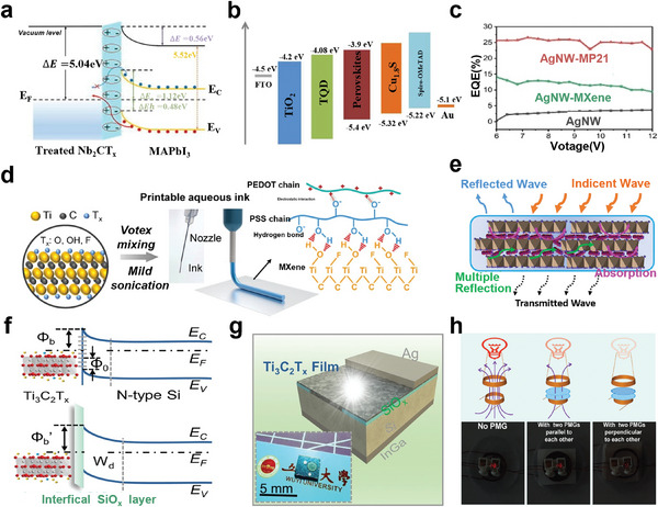
a) Energy level diagram of oxygen‐plasma‐treated Nb2CT x /MAPbI3. Reproduced with permission.[ 15 ] Copyright 20202, Wiley‐VCH. b) Energy diagram of each layer of SnO2:F(FTO)/TiO2/TQD/perovskites/Cu1.8S/2,2',7,7'‐tetrakis(N,N‐di‐p‐methoxyphenylamine)‐9,9'‐spiro‐bifluorene (Spiro‐OMeTAD)/Au PSCs. Reproduced with permission.[ 231 ] Copyright 2020, Wiley‐VCH. c) External quantum efficiency (EQE) of OLED devices using AgNW, AgNW–MXenes, and AgNW–MP21 (MXenes and PEDOT:PSS of mass ratio of 2:1) hybrid flexible transparent electrodes (FTEs). Reproduced with permission.[ 232 ] Copyright 2020, Elsevier. d) Schematic of MXene‐functionalized PEDOT:PSS ink for extrusion printing. Reproduced with permission.[ 16 ] Copyright 2021, Wiley‐VCH. e) Schematic of incident wave propagation through a printed product. Reproduced with permission.[ 9 b] Copyright 2021, American Chemical Society. f) Energy band diagram of a Ti3C2/Si heterojunction before and after interfacial modification, where Φ 0 is the surface potential, W d is the depletion width. g) Schematic illustration of the Ti3C2/SiO x /Si photodetector (PD), the inset is an actual device photograph. Reproduced with permission.[ 64 ] Copyright 2021, Wiley‐VCH. h) Polarization and switching effects of the microgratings to electromagnetic waves in a wireless generator device. Reproduced with permission.[ 23 ] Copyright 2022, American Chemical Society.