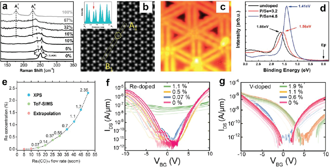
Figure 10.
Doping and alloying 2D materials for electrical applications. (a) Raman spectra of alloys showing a transition from the semiconducting 2H phase to the semimetallic 1T' phase as a function of increasing Te concentration. Adapted from ref 161. Copyright 2019 IOP Publishing Ltd. (b) ADF-STEM image and corresponding intensity profiles along the boxed region showing a P atom sitting at a Se site. (c) STM image of P-doped (sample bias: —1.0 V, size: 10 X 10 nm2). The hexagonal structure of remained intact after doping. (d) UPS of the undoped, lightly doped (P/Se flux ratio ≈3.2), and heavily doped (P/Se ≈4.5)-doped , showing a p-type behavior. Panels (b)—(d) were adapted with permission from ref 162. Copyright 2020 John Wiley & Sons, Inc. (e) The doping concentration of Re in from X-ray photoemission spectroscopy (XPS), secondary ion mass spectrometry (SIMS), and extrapolated points are plotted as a function of flow rate during growth. (f) Transfer characteristics of pristine and Redoped field-effect transistors. While ambipolar conduction in the pristine and lightly Redoped films is demonstrated, at higher Re concentrations device performance is degraded due to the increasing impurity scattering. Panels (e) and (f) were adapted and modified with permission from ref 164. Copyright 2020, Wiley-VCH. (g) Transfer characteristics of the pristine film at different drain voltages (1—5 V) display ambipolar conduction. However, the n-branch degrades as V concentration increases and transistors gradually become p-type. All transistors were on 50 nm ALD . Reproduced with permission from ref 165. Copyright 2021, Wiley-VCH.

