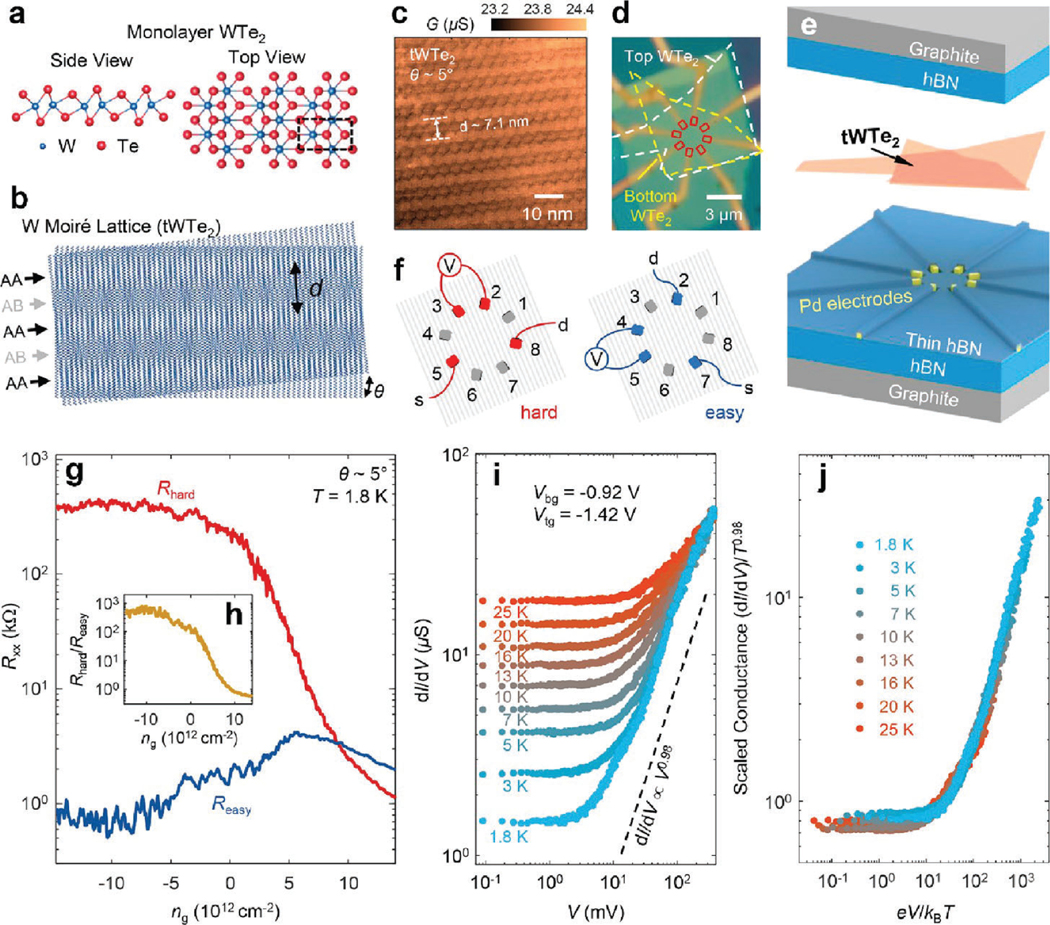
Figure 25.

Luttinger liquid behavior in moiré system. (a) The crystal structure for monolayer . The W atoms are sandwiched by two Te atom layers. From the top view, the W atoms (blue) form zigzag chains. The dashed square denotes the unit cell. (b) Moiré superlattice of , where only the W atoms are shown. The alternating AA and AB 1D stripes are illustrated. (c) conductive AFM image of a sample. (d) Optical image of a typical device, with the contact regions marked with red solid lines and the two layers of with yellow and white dashed lines, respectively. (e) Cartoon illustration of the device structure. From bottom to top: bottom graphite, bottom hBN, electrodes, thin hBN, , top hBN, and top graphite. (f) Measurement configuration for the hard and easy directions. The squares denote the contacts, and the gray lines indicate the moiré stripes. s, source; d, drain. (g) Four-probe resistance of the hard and easy direction shown in panel (f), measured at 1.8 K, as a function of the gate-induced doping density of the device. (h) The anisotropy ratio, with and in g, versus . (i) The across-wire differential conductance measured under different d.c. bias and temperature, with the doping fixed on the hole side. (j) Scaled differential conductance , plot against (same data in panel (i)), showing that all the data collapse into one curve. Adapted with permission from ref 453. Copyright 2022 Springer Nature.
