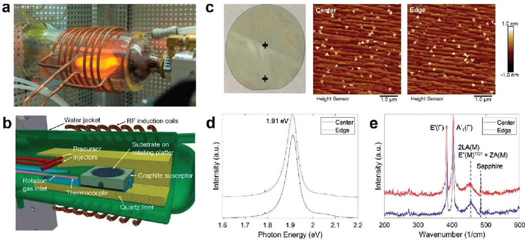
Figure 9.
MOCVD for epitaxial 2D TMD semiconductors. (a) photo and (b) schematic of horizontal cold wall MOCVD reactor used for TMD growth. (c) Surface morphology of monolayer grown on 2” c-plane sapphire at center and edge of the wafer (locations indicated by + in photo). Room temperature (d) PL and (e) Raman spectra obtained at the center and edge of the wafer show spatially uniform monolayer thickness across the wafer.

