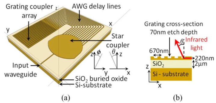
Figure 8.
(a) Two-dimensional beam scanner on SOI. A high-order grating is used in the ϕ direction and a low-order grating is used in the θ direction. (b) Cross-section of the grating coupler array. The SOI wafer has a 2 μm buried oxide layer and a 220 nm silicon top layer [39].

