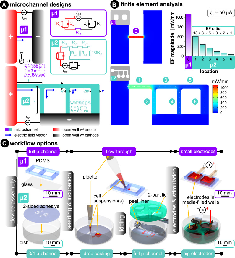
Figure 6.
(A) Device µ1 (violet) shows a top view of a simple rectangular microchannel that connects two open wells, each filled with excess media (mL in the wells and μL in the microchannel). Device µ2 (turquoise) shows a branching microchannel network that forms a current divider. Insets of the electrical equivalent circuit relate the microchannels to resistors and include the electrode–electrolyte interface of both the anode and cathode. (R = resistance, C = capacitance, and IDC = DC source). (B) Three-dimensional finite element analysis of both microchannel designs. The same input current (IDC = 50 μA) was used for both cases. The color scale and white arrows signifies the EF magnitude and direction, respectively. (C) Two different workflow options used in this paper allow for protocol flexibility. μ1 is made via soft lithography of molded polydimethylsiloxane (PDMS) that is irreversibly bonded to glass via air plasma exposure. μ2 is made by bonding the bottom side of a laser-structured double-sided adhesive to a Petri dish. Cell suspension(s) are flow-through seeded in μ1 and drop-casted in μ2. After cell seeding and growth in μ2, the adhesive’s top protective liner is removed, and an acrylic lid is added to complete the microchannels. Once the desired cell confluency is obtained, electrodes are added and stimulated in an incubated microscope.

