

Abstract
Transfer printing of small-molecular organic semiconductors often faces challenges due to surface adhesion mismatch. Here, we developed a sacrificing-layer-assisted transfer printing technique for the deposition of small-molecular thin films. High-boiling-point ethylene glycol (EG) was doped in aqueous solution poly(3,4-ethylenedioxythiophene) polystyrene sulfonate (PEDOT:PSS) as the sacrificing layer to manipulate residual water in film, which allowed chlorobenzene solution to spontaneously spread and form uniform film. The residual water guaranteed film delamination from the stamp, allowing for its transfer onto various substrates and seeding layers. As a proof of concept, laterally conductive organic photodetectors using recyclable EG-PEDOT:PSS electrodes and a small-molecular active layer were consecutively fabricated via transfer printing in ambient air. The resulting device exhibited a high on/off ratio of 711 and a fast rise time of 0.5 ms. Notably, the polymer electrode and the bulk heterojunction demonstrated unique repairability and recyclability.
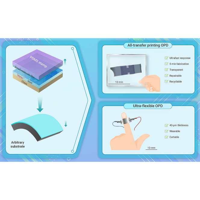
Graphical abstract
Public summary
-
•
Transfer printing of organic films avoids orthogonal solvents but strongly relies on surface energy.
-
•
A universal water-assisted transfer printing technique overcomes the mismatched interfacial adhesion.
-
•
Ethylene glycol was crucial to control the residual water to ease film delamination.
-
•
Fast, repairable, and recyclable all-organic photodetectors were fabricated via consecutive transfer printing.
-
•
Transfer printing based on the sacrificial layer allows film growth on arbitrary substrates.
Introduction
Organic semiconductors, featured with the advantages of light weight, flexibility, excellent tunability of optoelectronic properties, and ease of fabrication, have attracted extensive attention.1,2 Solution processes, including spin coating, inkjet printing, and blade coating, are popular and promising techniques for mass production of organic optoelectronic devices,3,4,5 compared with vacuum-based techniques that are expensive and complicated. However, constructing well-defined interfaces and geometrical patterns by solution processes poses challenges due to the intrinsic miscibility between the adjacent layers of organic semiconductors. For instance, the solution used to deposit an upper layer can dissolve the underlying layer. To address this issue, complicated solvent engineering, polymer additives, or post treatments are often adopted. However, they may degrade the performance of the devices.6,7,8
Transfer printing, which grows films on a mother substrate and then transfers them to the target dry substrate, has emerged as a feasible method to overcome the challenges associated with developing a multilayered organic semiconductor device using solution processes.9 Elastomeric stamps with low modulus and low surface energy such as polydimethylsiloxane (PDMS) are commonly used in transfer printing based on a direct contact mechanism. In the past decades, we have witnessed significant advancements made by this technique in assembling multiple dimensional structures of inorganic semiconductors on flexible or curved substrates.9
More recently, transfer printing has been applied to organic optoelectronic devices, such as organic light-emitting diodes (OLEDs) and organic photovoltaic cells (OPVs).10,11,12,13,14,15,16,17 For example, Bradley et al. spin-coated a layer of poly(3-hexylthiophene) (P3HT) polymer directly on a PDMS stamp, and then transfer-printed it onto an electron blocking layer, resulting in an enhancement of short-circuit photocurrent quantum efficiency.10 Kim et al. utilized a water-soluble sacrificial layer as a removable intermediate to ensure reliable and reproducible transfer printing of polymers, specifically poly(9,9-di-n-octylfluorene-alt-benzothiadiazole) (F8BT) and P3HT, for OLEDs and OPVs, respectively.16 In another recent example, a fluorescent polymer, poly(para-phenylene vinylene) (PPV), was transfer-printed onto a thermally activated delayed fluorescence (TADF) small molecule named (4,4′-sulfonylbis(4,1-phenylene))bis(9,9-dimethyl-9,10-dihydroacridine) (DMAC-DPS), to reduce interfacial quenching and enhance triplet exciton harvesting for improving device efficiency.15
Compared with polymers, small molecules are more promising for mass production of organic optoelectronic devices due to their simpler synthesis, higher purity, reproducibility, and well-defined chemical structures. However, conventional transfer printing technique that has been successfully adopted with polymers is not compatible with small molecules, probably due to the poor film-forming property and mismatched surface property. To exemplify this hypothesis, we tried to repeat the polymer-based transfer printing schemes proposed by using a well-known blue small-molecular TADF emitter called DMAC-DPS (Figure S1).14,18,19,20 As expected, the conventional transfer printing methods could not produce uniform films on substrates such as PDMS, silane-treated glass, or water. The mismatched interfacial adhesion prevented easy detachment of the DMAC-DPS film from hydrophilic glass, resulting in inferior transfer printing yields (Figure S2).
Similar to OPVs, organic photodetectors (OPDs) are also attractive devices due to high responsivity, tunable detection wavelengths, and vacuum-free solution processing.21 Typically, OPVs and OPDs both rely on bulk heterojunctions (BHJs), which spontaneously form intimate networks of donors and acceptors.22 Most of the high-performance OPDs are generally composed of polymer donors and small-molecular acceptors, although the polymers suffer from batch-to-batch deviation and purification challenges. All small-molecule photoconductors, on the other hand, hold great opportunities for large-area and integrated optoelectronic devices. Unlike the vertically stacked ones, the laterally photoconductive OPDs feature in-plane electrodes and active layer. Such simplified architecture can absorb light without experiencing optical loss to electrodes or waveguides, and enable the detection of gas and moisture more effectively.23
Herein, we demonstrated a universal transfer printing technique for fabricating small-molecule-based thin films. High-boiling-point ethylene glycol (EG) was doped into poly(3,4-ethylenedioxythiophene) polystyrene sulfonate (PEDOT:PSS) to form the sacrificial layer and control the water ingredient. The EG-PEDOT:PSS film facilitated the spontaneous spreading of hydrophobic small-molecule solutions, allowing for the formation of uniform films. The small-molecule film deposited on EG-PEDOT:PSS could be easily peeled off by PDMS and then transfer-printed onto arbitrary substrates or seeding layers. The all-transfer-printed OPDs, comprising the all-small-molecule active layer and recyclable EG-PEDOT:PSS electrodes, exhibited favorable performances, including a high on/off ratio of 711 and a rapid rise time of 0.5 ms.
Results
Transfer printing processes of small molecules
In Figures 1A–1E, a schematic flow of the transfer printing processes for depositing organic films on an arbitrary substrate is presented. The high-boiling EG dopant can efficiently protect water in film from rapid evaporation, which is crucial for successful transfer printing of small molecules. First, we optimized the EG doping concentration to 5 wt % because higher concentration would cause poor film formation, while lower concentration might lead to unsuccessful delamination of small molecules. The optimized EG-PEDOT:PSS aqueous solution was spin-coated on a mother glass to form a sacrificial layer (Figure 1A). When a water-immiscible organic solution with low surface energy was dropped onto the high-surface-energy water surface, the interfacial surface energy gradient would lead to the spontaneous surficial flow of organic solution toward the water-rich surface (Figure 1B), which is known as Marangoni flow.24 The spreading coefficient (S) determines the wetting behavior as follows25:
| (Equation 1) |
where γw, γo, and γw/o are the surface tension of water, organic solution, and water/organic solution interface, respectively (Figure 1B). If S > 0, the wetting and solution spreading are complete. If S < 0, the solution will form a lens-like geometry. When chlorobenzene (CB) is the solvent, S > 0 (71.6 − 33.6 − 37.4 = 0.6 mN/m).25 Therefore, the organic materials dissolved in CB can spread easily over the water-rich sacrificial layer, as confirmed by the instantaneous photos (Figure S3) when a CB droplet is dropped onto the sacrificial layer. The previous studies also verified the spontaneous film formation of polymers dissolved in CB on water substrate.19,26
Figure 1.

Schematic illustration of the transfer printing procedures
(A) Spin coating of EG-PEDOT:PSS aqueous solution on the mother glass.
(B) Spontaneous spreading of the solution on the water-rich EG-PEDOT:PSS.
(C) Spin coating of the solution to form a uniform active layer.
(D) Delamination of the active layer by a PDMS stamp.
(E) Printing of the active layer onto the target substrate.
(F and G) Schematic illustrations of the delamination of the luminescent layer DMAC-DPS from the mother glass substrate without (F) and with (G) the sacrificial layer (left) and the corresponding photos of the samples under ultraviolet (UV) light (right). Scale bar, 10 mm.
(H) Comparison of the works of adhesion between the interfaces of PDMS/active layer and active layer/substrate. The chemical structures of the active materials are illustrated in Figure S6.
After spin coating on the mother substrate (Figure 1C), the active material would be delaminated from the sacrificial layer by a PDMS stamp (Figure 1D). Generally, such delamination is dependent on the fracture energy (G) per unit between the small molecule and EG-PEDOT:PSS (Gsmall molecule/EG-PEDOT:PSS), and PDMS stamp and the small molecule (Gsmall molecule/PDMS).27 The fracture energy can be calculated by measuring the applied force per unit width (P) with a constant velocity during the peeling process as described in the following equation.28
| (Equation 2) |
where E, h, and θ are the elastic modulus, thickness of the PDMS, and the peeling angle, respectively. The first term in Equation 2 is negligible under the assumption of high tensile stiffness and low bending stiffness. The peeling angle is about 90°. We employed the highly emissive small-molecule DMAC-DPS as a representative example since the processes and defects are easily visible under UV lamp. To ensure complete delamination, GPDMS/DMAC-DPS should be greater than GDMAC-DPS/EG-PEDOT:PSS. As shown in Figures 1F and 1G, GPDMS/DMAC-DPS and GDMAC-DPS/EG-PEDOT:PSS were measured by peeling off the DMAC-DPS film from glass and EG-PEDOT:PSS layer, respectively. In the former case, delamination occurred at the interface between PDMS and DMAC-DPS owing to the strong interface between glass and DMAC-DPS. The measured GDMAC-DPS/PDMS was 5.0 J/m2, which is almost an order of magnitude higher than GDMAC-DPS/EG-PEDOT:PSS (0.6 J/m2). This indicates that DMAC-DPS can be easily peeled off from the sacrificial layer by PDMS. The result can be ascribed to the dramatically decreased van der Waals interactions and interfacial friction between the water-rich EG-PEDOT:PSS and the hydrophobic aromatic DMAC-DPS, which is consistent with the previous studies.29,30
To guarantee transfer printing of the active layer from PDMS to the target substrate, GDMAC-DPS/substrate should be greater than GPDMS/DMAC-DPS. However, directly measuring GDMAC-DPS/substrate seems to be daunting, owing to the strong fracture energy between the small-molecular film and the target substrate. Instead, we calculated the interfacial work of adhesion (W), which is generally proportional to the fracture energy (Note S1).31 To guarantee the complete transfer printing of DMAC-DPS from PDMS to the target substrate, the works of adhesion between the target substrates and DMAC-DPS (WDMAC-DPS/substrate) should be higher than those between DMAC-DPS and PDMS (WDMAC-DPS/PDMS), respectively. The works of adhesion could be rationally quantified by the reported method with two different testing droplets (Note S2 and Table S1).15,32
Based on the contact angles (Figure S4), the calculated surface energies and works of adhesion are summarized in Tables S2 and S3, respectively. Five ubiquitous flexible or curved objects were chosen as the target substrates (Figures 2A–2E). As shown in Figure 1H, the values of WDMAC-DPS/substrate (81–374 mJ/m2) are much higher than that of WPDMS/DMAC-DPS (26.2 mJ/m2), indicating that the transfer printing of DMAC-DPS from the PDMS stamp to various target substrates can be successfully achieved. The flow of transfer printing processes is presented in Figure S5, which could be accomplished within 3 min under ambient air conditions.
Figure 2.

Transfer printing of the small molecular emitters on the different substrates
(A–E) Photos of the red, green, and blue (RGB) small-molecule strips transfer-printed on (A) plastic bottle, (B) pop-top can, (C) glass bottle, (D) plastic package, and (E) cardboard under 365-nm UV light, respectively. The BGR strips were composed of DMAC-DPS, 4CzIPN, and Ir(MDQ)2(acac) emitters, respectively. 4CzIPN and Ir(MDQ)2(acac) were doped in mCP host with the concentrations of 10 wt % and 5 wt %, respectively. The scale bars in the photos and the corresponding insets are 10 and 5 mm, respectively.
(F) PL spectra of DMAC-DPS (B), DMAC-DPS/4CzIPN (B/G) and DMAC-DPS/4CzIPN/Ir(MDQ)2(acac) (B/G/R) stacks after transfer printing, excited at 380 nm. Inset: photos of the striped films under 365-nm UV lamp. Scale bar, 10 mm.
(G) Optical microscopy images of DMAC-DPS film transferred onto a glass under white light and UV light, respectively. The scratches at the bottom of the images were deliberately created for comparison.
The uniform DMAC-DPS film was obtained on a glass substrate after transfer printing (Figure 2G). The photoluminescence profile of DMAC-DPS remained identical to that of the film fabricated by spin coating (Figure S2A). In addition, such transfer printing assisted by the sacrificial layer provides a considerably high yield (approaching to 100%), which is rarely achieved by any other transfer printing methods (Figure S2B).
To demonstrate the transfer printing assisted by the sacrificial layer as a universal and versatile technique to deposit thin films for optoelectronic applications, different types of materials, including small-molecular 4CzIPN for OLEDs and non-fullerene acceptor T8Me for OPVs, as well as dendrimer 4CzDMAC-DPS, polymer PCzDP-15, and red quantum dot (QD-R), were respectively evaluated. Owing to the differences in interfacial adhesion as illustrated in Figure 1H, all these films can be peeled off from EG-PEDOT:PSS and subsequently transfer-printed onto the five different target substrates indicated in Figure 2. The identical steady-state and transient spectral profiles of the films fabricated by spin coating and transfer printing imply no substantial change of the optoelectronic properties (Figure S6 and Table S4). Furthermore, blue, green, and red small-molecular strips can be easily transfer-printed (Figures 2A–2E), regardless of the surface properties of the target substrates. This characteristic makes it feasible to create diverse film stacks and patterns on packages or textiles (Figures S7 and S8). For example, different film stacks can be sequentially transfer-printed on the glass substrate, leading to overlapping emission (Figure 2F).
Influence of EG in PEDOT:PSS on transfer printing
The presence of EG doped in PEDOT:PSS is found to be crucial for achieving high-yield transfer printing. The additive EG, with a high boiling point of 197°C, effectively slows down the evaporation of residual water from PEDOT:PSS after spin coating. Previous studies have verified that alcohol monolayers can suppress the escape of water molecules.33,34 To confirm the existence of residual water in EG-PEDOT:PSS, we compared the delamination behavior of DMAC-DPS films spin-coated from two different solvents: CB and tetrahydrofuran (THF), which is miscible with water. After spin coating these two solutions on EG-PEDOT:PSS, the delamination tests were conducted using PDMS (Figures 3A and 3B). It is evident that DMAC-DPS from CB solution can form a uniform film on EG-PEDOT:PSS with the distinct interface, as confirmed by the cross-sectional scanning electron microscopy (SEM) image in Figure 3A. In contrast, DMAC-DPS from THF solution partially mixed with the underlying EG-PEDOT:PSS layer (Figure 3D), and cannot be delaminated by PDMS due to the strong interfacial adhesion (inset of Figure 3B).
Figure 3.

Cross-sectional images of film stacks and the evolution of the residual water in the sacrifial layer
(A and B) Cross-sectional SEM images of DMAC-DPS spin-coated from (A) CB and (B) THF solutions on EG-PEDOT:PSS. Inset: Photos of DMAC-DPS as cast on glass and transferred to PDMS under UV light, respectively.
(C) Time-dependent FTIR absorption spectra of EG-PEDOT:PSS.
(D) FTIR absorption of liquid and vaporous water at different time intervals.
(E and F) Time-dependent conductivities of EG-PEDOT:PSS (E) and pristine PEDOT:PSS (F) with 1-mm-width channel over two separated indium tin oxide (ITO) electrodes.
To investigate water evaporation from the as-cast EG-PEDOT:PSS, we measured real-time microscope Fourier transform infrared (FTIR) absorption spectra of the film, as shown in Figures 3C and 3D. During the initial 5 min (Figure S9), the fast water evaporation at the film’s surface led to the irregular spectral changes. Subsequently, the FTIR spectra showed a clear evolution in intensities and peak positions. The bands from 3,000 to 3,400 cm−1 and 3,500 to 3,800 cm−1 corresponded to the stretching and bending vibrations of O-H in liquid and vaporous water,35,36 respectively. From 6 to 9 min, the signals of liquid water slightly increased, probably due to the migration of bulk water residing in EG-PEDOT:PSS to the film’s surface. Afterward, the residual liquid water gradually decreased from 9 to 16 min due to the slow evaporation process. Therefore, the signals of vaporous water gradually increased and then reached saturation in the final 3 min. Besides, the wavenumbers of both states shifted to higher values, indicating a decrease in the hydrogen network in water.37 It is worth noting that the presence of residual water can ensure the complete delamination of organic films within approximately 15 min after spin coating EG-PEDOT:PSS at 25°C and 60% relative humidity. In contrast, the FTIR signal of PEDOT:PSS without EG remained unchanged even after 3 min of spin coating (Figure S10), verifying the fast water evaporation and drying process in the absence of EG. Consequently, the active layers cannot be successfully peeled off from PEDOT:PSS.
To further explore the effect of residual water, conductivity tests were performed on the EG-PEDOT:PSS film. As depicted in Figure 3E, the conductivity of EG-PEDOT:PSS film continuously increased from 165 to 226 S/cm over a period of 1,000 s, indicating the slow evaporation of residual water that separated the conductive polymer networks. This observation aligns with the FTIR measurement. However, the conductivity of PEDOT:PSS without EG remained relatively unchanged at around 0.8 S/cm (Figure 3F), implying no trace of residual water. Compared with the as-cast PEDOT:PSS film, the significantly improved conductivity of PEDOT:PSS with EG additive is ascribed to the well-known effects of chain reordering and conformational changes.38 Accordingly, the residual water plays a critical role by imparting weak adhesion between EG-PEDOT:PSS and the organic layer, facilitating the subsequent delamination process.
All-transfer-printing OPDs
As a proof of concept, we employed the universal transfer printing technique to construct all-transfer-printing organic photodetectors. Figure 4A presents a schematic illustration of the fabrication procedures. In such a laterally conductive architecture, EG-PEDOT:PSS, serving as the semitransparent electrode, was spin-coated on a PDMS stamp and then cut into a desired strip, which was further transfer-printed onto the target glass substrate. To define the active area, the EG-PEDOT:PSS film was carefully scratched by a scalpel to form two separated electrodes and a single channel (3 mm in length and 30 μm in width) (Figures S11A and S11B). All-small-molecule BHJ-based active layer, including benzo[1,2-b′:4,5-b′]dithiophene (BDT) based p-type donor (BDTT-TR)39 and n-type fullerene acceptor PC61BM with the mass ratio of 1:1, was transfer-printed on the channel to construct OPDs. The single-channel-based OPD can be accomplished within 5 min in air by the two-step transfer printing processes. The chemical structures and corresponding absorption spectra of BDTT-TR and PC61BM are provided in Figure S12, while the energy level alignments of the materials are schematically illustrated in Figure 4C.
Figure 4.

Transfer printing of all-organic photodetectors and the performances
(A and B) Schematic flow of device fabrication of (A) single-channel-based and (B) interdigital-electrode-based photoconductors.
The corresponding device photos are illustrated at the right-hand side, respectively.
(C) Energy level alignment of EG-PEDOT:PSS, BDTT-TR, and PC61BM obtained from the literature.39
(D) Current-voltage curves of the devices under dark and 528-nm LED illumination.
(E) Temporal photoresponse of the devices at a bias of 5 V.
(F) Photocurrent and responsivity versus irradiance under 532-nm laser illumination, biased at 5 V.
(G) Noise density as a function of frequency at different voltages.
(H) Responsivity, external quantum efficiency, and specific detectivity curves.
The dark current should be low enough to reduce energy consumption and enhance signal extraction. Unfortunately, the single-channel-based OPDs exhibited a relatively high dark current of 1.9 nA at 10 V (Figure 4D), and thus a small on/off ratio of 6.1. This result is partially attributed to the residual conductive path in the channel created during the mechanical scratching process. To address this issue, we introduced a 1,064-nm laser to ablate the PEDOT:PSS film and customize the interdigital electrode with a total length of 67.1 mm and a width of 100 μm (Figures S11C and S11D). The layout of the interdigital electrode is shown in Figure S20. The width of the channel can be significantly narrowed by introducing femtosecond laser ablation,40 taking advantage of the strong absorbance of the EG-PEDOT:PSS film at 1,064 nm (Figure S13). However, these devices rendered high dark currents, regardless of whether the active layer was spin-coated or transfer-printed (Figures S14A and S14B). Therefore, a black ink layer, which is highly absorptive and can produce extra heat to guarantee the complete ablation of EG-PEDOT:PSS, was inserted as a seeding layer beneath the EG-PEDOT:PSS electrode (Figure 4D). The device with both the spin-coated active layer and the black-ink-based seeding layer did not function well due to the interfacial mixing effect of non-orthogonal solvents used (Figure S14C). In contrast, the transfer-printed device with the seeding layer exhibited obvious photoresponse (Figure S14D) under white LED illumination (Figure S15). Due to the elimination of residual conductive path, the interdigital-electrode-based device exhibited a dark current as low as 0.14 nA at a 10 V bias (Figure 4D), resulting in a two orders of magnitude higher on/off ratio of 711 compared with the single-channel-based device. In addition, the devices were semitransparent (Figure S16), making them suitable for integration in under-display sensors for smartphones or smart windows for buildings.41
The response time is a critical indicator reflecting the performance of optical sensors. Figure 4E illustrates the transient photocurrent response of the two different devices under a 528-nm light source. The rise/fall times (trise/tfall) are 0.7/2.8 and 0.5/1.4 ms, respectively, for the single-channel-based and the interdigital-electrode-based devices. The fast response time out-performs those of previously reported organic lateral photodetectors,42,43 and is even comparable with those of the state-of-the-art perovskite photodetectors and 2D materials-based detectors (Table S5).44,45,46,47 The fast photoresponse indicates the efficient exciton dissociation and charge carrier extraction in the all-small-molecule-based active layer, primarily attributed to the large donor-acceptor energy offsets (Figure 4C) and high carrier mobilities.39
The photocurrent-light-intensity-responsivity (R) curves of the interdigital-electrode-based device are shown in Figure 4F. The photocurrent increased and the responsivity decreased with the increasing incident light intensity from 2.3 × 10⁻⁴ to 9.2 mW/cm2. This trend is consistent with typical OPDs.48 The noise density (In) as a function of frequency at different biased voltages is compared in Figure 4G, delivering a low noise down to 10−11 A/Hz1/2. Furthermore, the responsivity, external quantum efficiency (EQE), and specific detectivity under different wavelengths are illustrated in Figure 4H. The device showed a broadband photoresponse covering the UV-visible region from 320 to 700 nm, benefiting from the excellent absorption of the all-small-molecule active layer (Figure S12C). As a result, the device achieved a maximum responsivity of 17 mA/W at 650 nm, along with a maximum EQE of 0.033% at 350 nm and a maximum specific detectivity of 1.5 × 10⁸ Jones at 650 nm. Moreover, the device without any encapsulation demonstrated considerable stability during relatively long-term operation and storage (Figure S17), which is very competitive compared with the air-sensitive vertical-stacked OPDs with metal electrodes.
The simple lateral configuration of the OPD allows recycling of the polymer electrode EG-PEDOT:PSS by washing away the photoactive layer with dichloromethane (Figure S18). Furthermore, any broken or lacerated polymer electrode, such as those cut off by a scalpel, can be easily repaired by transfer printing another piece of EG-PEDOT:PSS (Figure S19). The repairable OPDs have potential applications in bioelectronic and wearable electronics, where frequent damage may occur due to mechanical motion or protracted contact with bio-tissue.49
Ultra-flexible OPDs
Since transfer printing technique can deposit both the polymer electrode and the active layer on arbitrary substrates without utilizing any brittle metal films, we can easily customize ultra-flexible OPDs, which are highly desired for smart and unobtrusive photodetection on common objects, e.g., the human body. First, a semitransparent device was fabricated on a polyethylene terephthalate (PET) substrate (inset of Figure 5A), demonstrating an on/off ratio of 5.2 at 10 V comparable to the rigid device (Figure 5A). Remarkably, the response times (trise/tfall) of the flexible device were as small as 1.4/0.3 ms, respectively (Figure 5B). To further construct the ultra-flexible OPDs, the interdigital-electrode-based device was transfer-printed and laser-patterned on an ultrathin scotch tape with only 40-μm thickness (Figure 5C). The free-standing tape-based OPD can be adhered onto and wrapped around the human finger, showing stable photoresponse with a reasonable on/off ratio of 12.4 under flashlight illumination (Figure 5D).
Figure 5.

Performance of the laterally conductive flexible organic photodetectors
(A) Current-voltage curves of the PET-based flexible device under dark and illumination by a 528-nm LED (96 mW/cm2). Inset: Photo of the flexible device.
(B) Temporal photoresponse of the flexible device under 528-nm LED illumination (51 mW/cm2) at a bias of 5 V.
(C) Photo of the ultra-flexible and wearable OPD adhered on a forefinger. Inset: Schematic diagram of the device architecture.
(D) Temporal photoresponse of the wearable device under flashlight at 30-V bias.
(E and F) Temporal photoresponse and photos of the flexible device driven at 10 V before (E) and after (F) being cut off by scissors, illuminated by a flashlight (21.3 mW/cm2). Owing to the simple single-channel-based configuration, cutting off the PET-based device in any direction simply shortens the width of electrode and/or channel, i.e., the size of the active area. Due to the robust configuration of the laterally conductive devices, the remaining device still preserves the detector functions without short or open circuits. Scale bar, 10 mm.
Benefiting from the simple single-channel-based configuration, the PET-based device can be cut into pieces (Figures 5E and 5F). Even after cutting, the separated devices maintained stable photoresponse with reduced currents but almost identical on/off ratios of ∼5. This demonstrates the promise of integrating these simple OPDs with complex objects to survive unintentional damage, which could be fatal for vertically structured OPDs with significantly thinner active layers.
Discussion
We demonstrated a unique and universal transfer printing technique based on the sacrificial layer, enabling the easy transfer of common organic materials from the water-rich EG-PEDOT:PSS surface onto arbitrary substrates or seeding layers. By incorporating the high-boiling EG additive into PEDOT:PSS aqueous solution, the technique efficiently protected water in the film from rapid evaporation. Furthermore, the residual water dramatically reduced van der Waals interactions and thus ensured the complete delamination of hydrophobic aromatic films. As a proof of concept, we fabricated all-transfer-printed laterally conductive OPDs with two EG-PEDOT:PSS electrodes and an all-small-molecule photoactive layer in the channel. These devices, without any encapsulation, exhibited a low dark current of 1.4 × 10⁻¹⁰ A at 10 V, a high on/off ratio of 711, and a fast rise time of only 0.5 ms. Due to the ease of device fabrication on the arbitrary substrates, the flexible OPDs on common substrates, such as PET and even the ubiquitous scotch tape (40-μm thick), demonstrated similar device performance to rigid devices. Furthermore, the single-channel-based flexible device can be recycled and repaired after damage and even being split into sub-devices. This transfer printing technique will pave a path toward more reliable and affordable organic devices for sensing, imaging, and biological applications.
Materials and methods
See supplemental information for details.
Acknowledgments
We thank Prof. Yinhua Zhou and Dr. Tiefeng Liu at Huazhong University of Science and Technology for technical discussion and Prof. Longjian Xue, Dr. Qian Li., Dr. Ruijie Ming, Ms. Lisi Zhan, Ms. Yiwen Yang, and Mr. Jiale Li at Wuhan University for the discussions and measurements. This research was financially supported by the National Natural Science Foundation of China (No. 62175189), the Shenzhen Science and Technology Program (KQTD20170330110107046). G.X. acknowledged funding support from the Program for Promoting Academic Collaboration and Senior Talent Fostering between China and Canada, Australia, New Zealand, and Latin America (2021-109), and the Joint China-Sweden Mobility Programme (No. 52211530052).
Author contributions
Y.T. completed the transfer printing experiments and manuscript draft. R.L. and Q.L. carried out the measurements of photodetectors. R.S. and J.M. synthesized the non-fullerene acceptor. G.X. conceived the idea. G.X. and C.Y. supervised, organized, and revised the manuscript. All authors have read and agreed to the published version of the manuscript.
Declaration of interests
The authors declare no competing interests.
Published Online: June 15, 2023
Footnotes
It can be found online at https://doi.org/10.1016/j.xinn.2023.100460.
Contributor Information
Qianqian Lin, Email: q.lin@whu.edu.cn.
Chuluo Yang, Email: clyang@szu.edu.cn.
Guohua Xie, Email: guohua.xie@whu.edu.cn.
Lead contact website
Supplemental information
References
- 1.Chow P.C.Y., Someya T. Organic photodetectors for next-generation wearable electronics. Adv. Mater. 2020;32 doi: 10.1002/adma.201902045. [DOI] [PubMed] [Google Scholar]
- 2.Zhang Z., Wang W., Jiang Y., et al. High-brightness all-polymer stretchable LED with charge-trapping dilution. Nature. 2022;603:624–630. doi: 10.1038/s41586-022-04400-1. [DOI] [PubMed] [Google Scholar]
- 3.Fabiano S., Facchetti A. Stretchable helix-structured fibre electronics. Nat. Electron. 2021;4:864–865. [Google Scholar]
- 4.Iqbal H.F., Ai Q., Thorley K.J., et al. Suppressing bias stress degradation in high performance solution processed organic transistors operating in air. Nat. Commun. 2021;12:2352. doi: 10.1038/s41467-021-22683-2. [DOI] [PMC free article] [PubMed] [Google Scholar]
- 5.Wang S., Zhang H., Zhang B., et al. Towards high-power-efficiency solution-processed OLEDs: material and device perspectives. Math. Sci. Eng. R. 2020;140:100547. [Google Scholar]
- 6.Gao Y., Tang Y., Liu H., et al. Thermally activated delayed fluorescent polymer- assisted morphological control on perfluorinated ionomer enriched surface and exciton harvesting for phosphorescent organic light-emitting devices. Dyes Pigments. 2020;183:108718. [Google Scholar]
- 7.Park J., Yoon H., Kim G., et al. Highly customizable all solution–processed polymer light emitting diodes with inkjet printed Ag and transfer printed conductive Polymer electrodes. Adv. Funct. Mater. 2019;29:1902412. [Google Scholar]
- 8.Tsougeni K., Vourdas N., Tserepi A., et al. Mechanisms of oxygen plasma nanotexturing of organic polymer surfaces: from stable super hydrophilic to super hydrophobic surfaces. Langmuir. 2009;25:11748–11759. doi: 10.1021/la901072z. [DOI] [PubMed] [Google Scholar]
- 9.Park J., Lee Y., Lee H., Ko H. Transfer printing of electronic functions on arbitrary complex surfaces. ACS Nano. 2020;14:12–20. doi: 10.1021/acsnano.9b09846. [DOI] [PubMed] [Google Scholar]
- 10.Chen L., Degenaar P., Bradley D.D.C. Polymer transfer printing: application to layer coating, pattern definition, and diode dark current blocking. Adv. Mater. 2008;20:1679–1683. [Google Scholar]
- 11.Huang J.-H., Ho Z.-Y., Kuo T.-H., et al. Fabrication of multilayer organic solar cells through a stamping technique. J. Mater. Chem. 2009;19:4077–4080. [Google Scholar]
- 12.Kim J.B., Guan Z.-L., Lee S., et al. Modular construction of P3HT/PCBM planar-heterojunction solar cells by lamination allows elucidation of processing–structure–function relationships. Org. Electron. 2011;12:1963–1972. [Google Scholar]
- 13.Kim N., Kang H., Lee J.H., et al. Highly conductive all-plastic electrodes fabricated using a novel chemically controlled transfer-printing method. Adv. Mater. 2015;27:2317–2323. doi: 10.1002/adma.201500078. [DOI] [PubMed] [Google Scholar]
- 14.Mohapatra A., Singh A., Abbas S.A., et al. Bilayer polymer solar cells prepared with transfer printing of active layers from controlled swelling/de-swelling of PDMS. Nano Energy. 2019;63:103826. [Google Scholar]
- 15.Tang Y., Gao Y., Xie G., Yang C. Transfer printing of polymer light-emitting devices with a small molecular seeding layer featuring thermally activated delayed fluorescence for triplet harvesting. Nanoscale Horiz. 2020;5:144–149. [Google Scholar]
- 16.Yim K.-H., Zheng Z., Liang Z., et al. Efficient conjugated-polymer optoelectronic devices fabricated by thin-film transfer-printing technique. Adv. Funct. Mater. 2008;18:1012–1019. [Google Scholar]
- 17.Zhou Y., Khan T.M., Shim J.W., et al. All-plastic solar cells with a high photovoltaic dynamic range. J. Mater. Chem. 2014;2:3492–3497. [Google Scholar]
- 18.Kim T.-H., Cho K.-S., Lee E.K., et al. Full-colour quantum dot displays fabricated by transfer printing. Nat. Photonics. 2011;5:176–182. [Google Scholar]
- 19.Noh J., Jeong S., Lee J.Y. Ultrafast formation of air-processable and high-quality polymer films on an aqueous substrate. Nat. Commun. 2016;7:12374. doi: 10.1038/ncomms12374. [DOI] [PMC free article] [PubMed] [Google Scholar]
- 20.Xiong S., Li L., Qin F., et al. Universal strategy to reduce noise current for sensitive organic photodetectors. ACS Appl. Mater. Interfaces. 2017;9:9176–9183. doi: 10.1021/acsami.6b16788. [DOI] [PubMed] [Google Scholar]
- 21.Liu M., Fan Q., Yang K., et al. Broadband photomultiplication-type polymer photodetectors and its application in light-controlled circuit. Sci. China Chem. 2022;65:1642–1649. [Google Scholar]
- 22.Zhao Z., Xu C., Ma Y., et al. Filter-free narrowband photomultiplication-type planar heterojunction organic photodetectors. Adv. Funct. Mater. 2022;33:2212149. [Google Scholar]
- 23.Lin T., Wang J. Strategies toward high-performance solution-processed lateral photodetectors. Adv. Mater. 2019;31 doi: 10.1002/adma.201901473. [DOI] [PubMed] [Google Scholar]
- 24.Poulard C., Damman P. Control of spreading and drying of a polymer solution from marangoni flows. Europhys. Lett. 2007;80:64001. [Google Scholar]
- 25.Demond A.H., Lindner A.S. Estimation of interfacial tension between organic liquids and Water. Environ. Sci. Technol. 1993;27:2318–2331. [Google Scholar]
- 26.Colberts F.J.M., Wienk M.M., Heuvel R., et al. Bilayer-ternary polymer solar cells fabricated using spontaneous spreading on water. Adv. Energy Mater. 2018;8:1802197. [Google Scholar]
- 27.Meitl M.A., Zhu Z.-T., Kumar V., et al. Transfer printing by kinetic control of adhesion to an elastomeric stamp. Nat. Mater. 2005;5:33–38. [Google Scholar]
- 28.Kendall K. Thin-film peeling - the elastic term. J. Phys. D Appl. Phys. 1975;8:1449–1452. [Google Scholar]
- 29.Fan Z., Ho J.C., Jacobson Z.A., et al. Wafer-scale assembly of highly ordered semiconductor nanowire arrays by contact printing. Nano Lett. 2008;8:20–25. doi: 10.1021/nl071626r. [DOI] [PubMed] [Google Scholar]
- 30.Jeong J.W., Yang S.R., Hur Y.H., et al. High-resolution nanotransfer printing applicable to diverse surfaces via interface-targeted adhesion switching. Nat. Commun. 2014;5:5387. doi: 10.1038/ncomms6387. [DOI] [PubMed] [Google Scholar]
- 31.Packham D.E. Surface energy, surface topography and adhesion. Int. J. Adhesion Adhes. 2003;23:437–448. [Google Scholar]
- 32.Wu S. Calculation of interfacial tension in polymer systems. J. polym. sci. C. Polym. symp. 2007;34:19–30. [Google Scholar]
- 33.La Mer V.K., Healy T.W. Evaporation of water: its retardation by monolayers. Science. 1965;148:36–42. doi: 10.1126/science.148.3666.36. [DOI] [PubMed] [Google Scholar]
- 34.Mozafari A., Mansouri B., Chini S.F. Effect of wind flow and solar radiation on functionality of water evaporation suppression monolayers. Water Resour. Manag. 2019;33:3513–3522. [Google Scholar]
- 35.Roscoe J.M., Abbatt J.P.D. Diffuse reflectance FTIR study of the interaction of alumina surfaces with ozone and water vapor. J. Phys. Chem. A. 2005;109:9028–9034. doi: 10.1021/jp050766r. [DOI] [PubMed] [Google Scholar]
- 36.Movasaghi Z., Rehman S., ur Rehman D.I. Fourier Transform Infrared (FTIR) spectroscopy of biological tissues. Appl. Spectrosc. Rev. 2008;43:134–179. [Google Scholar]
- 37.Asprion N., Hasse H., Maurer G. FT-IR spectroscopic investigations of hydrogen bonding in alcohol–hydrocarbon solutions. Fluid Phase Equil. 2001;186:1–25. [Google Scholar]
- 38.Ouyang J., Xu Q., Chu C.-W., et al. On the mechanism of conductivity enhancement in poly(3,4-ethylenedioxythiophene):poly(styrene sulfonate) film through solvent treatment. Polymer. 2004;45:8443–8450. [Google Scholar]
- 39.Sun R., Wu Y., Guo J., et al. High-efficiency all-small-molecule organic solar cells based on an organic molecule donor with an asymmetric thieno[2,3-f] benzofuran unit. Sci. China Chem. 2020;63:1246–1255. [Google Scholar]
- 40.Jiang Q., Chen L., Liu J., et al. Periodic transparent nanowires in ITO film fabricated via femtosecond laser direct writing. Opto-Electron. Sci. 2023;2:220002. [Google Scholar]
- 41.Tian W., Zhai T., Zhang C., et al. Low-cost fully transparent ultraviolet photodetectors based on electrospun ZnO-SnO2 heterojunction nanofibers. Adv. Mater. 2013;25:4625–4630. doi: 10.1002/adma.201301828. [DOI] [PubMed] [Google Scholar]
- 42.Han T., Xu Y., Shou M., et al. Energy level gradient trapping based on different work functions of ZnO enhancing response and stablity for lateral photodetectors. Org. Electron. 2020;86:105883. [Google Scholar]
- 43.Tong S., Chen S.C., Xu K.Y., et al. Large-scale roll-to-roll printed, flexible and stable organic bulk heterojunction photodetector. NPJ Flex. Electron. 2018;643:7–13. [Google Scholar]
- 44.Feng J., Gong C., Gao H., et al. Single-crystalline layered metal-halide perovskite nanowires for ultrasensitive photodetectors. Nat. Electron. 2018;1:404–410. [Google Scholar]
- 45.Liu Y., Ye H., Zhang Y., et al. Surface-tensioncontrolled crystallization for high-quality 2D perovskite single crystals for ultrahigh photodetection. Matter. 2019;1:465–480. [Google Scholar]
- 46.Tang L., Teng C., Luo Y., et al. Confined van der Waals epitaxial growth of two-dimensional large single-crystal In(2)Se(3) for flexible broadband photodetectors. Research. 2019;2019:2763704. doi: 10.34133/2019/2763704. [DOI] [PMC free article] [PubMed] [Google Scholar]
- 47.Yang Z., Deng Y., Zhang X., et al. High-performance single-crystalline perovskite thin-film photodetector. Adv. Mater. 2018;30:1704333. doi: 10.1002/adma.201704333. [DOI] [PubMed] [Google Scholar]
- 48.Konstantatos G., Clifford J., Levina L., Sargent E.H. Sensitive solution-processed visible-wavelength photodetectors. Nat. Photonics. 2007;1:531–534. [Google Scholar]
- 49.Zou Z., Zhu C., Li Y., et al. Rehealable, fully recyclable, and malleable electronic skin enabled by dynamic covalent thermoset nanocomposite. Sci. Adv. 2018;4 doi: 10.1126/sciadv.aaq0508. [DOI] [PMC free article] [PubMed] [Google Scholar]
Associated Data
This section collects any data citations, data availability statements, or supplementary materials included in this article.