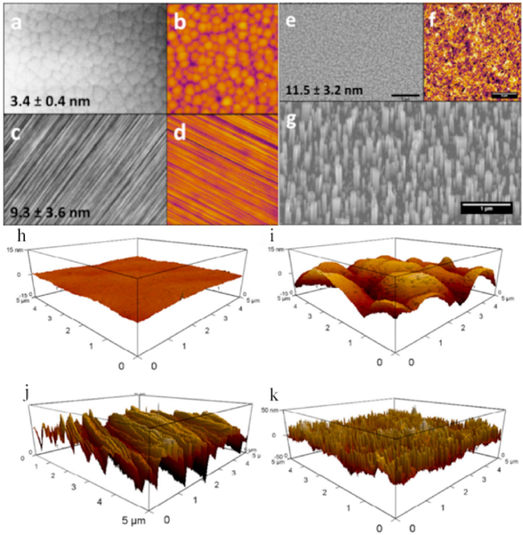
Fig. 4.
GaN can be etched into different nanostructures by different methods. (a) and (b) for planar surface, (c) and (d) for polished surface, and (e) and (f) for etched surfaces. (a), (c), (e), and (g) were SEM images. (b), (d), and (f) were AFM images. The values listed at the bottom left of the SEM images were RMS roughness. (g) The substrate is positioned at an angle To accurately represent the aspect ratios of the nanowires [52]. Four GaN surface morphologies were demonstrated using 3D AFM. (h)lateral steppes GaN, (i) spiral hillocks GaN, (j) mechanically polished GaN, and (k) photochemically etched GaN. Height range 30 nm in (h–j), 100 nm in (d) [53].

