Figure 5.

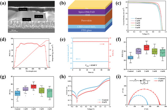
a) The cross‐section SEM image of the fabricated PSCs. b) The structure schematic image of a typical PSC device. (The device structure: FTO/PAPT‐modified SnO2/perovskite/OAI/Spiro‐OMeTAD/Au). c) J–V curves of the champion PSCs based on the different amounts of periodic acid treatments. d) EQE spectra for the PSCs based on the PAPT‐modified SnO2 film. e) Steady‐state photocurrent measurement of the champion PSC based on the PAPT‐modified SnO2 film. The applied bias voltage was 0.949 V, which was the voltage at the maximum power point. f) PCE and g) FF statistic distributions of the PSCs with different amounts of periodic acid treatments. h) Dark I–V curves of the PSCs based on the pristine SnO2 and PAPT‐modified SnO2 films. i) Nyquist plots of the PSCs based on the pristine SnO2 and PAPT‐modified SnO2 films, which was measured at a bias potential of 1.0 V in the frequency range of 1 MHz to 0.1 Hz in the dark.
