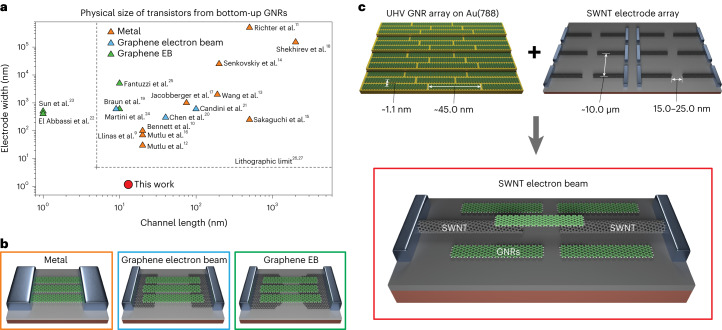
Fig. 1. Size scaling in bottom-up GNR-based transistors with various geometries.
a, Comparison of the physical size of transistors from GNRs with different contact strategies: metal electrodes9–18 (orange), EBL-defined graphene electrodes19–21 (blue), EB-formed graphene electrodes22–25 (green) and EBL-defined SWNT electrode (red; this work). The squares represent surface-polymerized GNRs in an ultrahigh vacuum; the triangles represent solution-polymerized GNRs; the circles represent CVD-synthesized GNRs. b, Schematic of the transistors of typical bottom-up GNR transistors with metal electrodes (left), EBL-defined graphene electrodes (middle) and EB-formed graphene electrodes (right). c, Ultimately scaled SWNT electrodes for contacting bottom-up GNRs. Schematic of the ultrahigh vacuum (UHV)-synthesized GNR array parallel to the Au(788) terraces (top left). Schematic of the parallel SWNT electrode array on a SiO2 substrate (top right). Schematic of a single-GNR-based transistor with SWNTs as ultimately scaled electrodes (bottom). For clarity, only the GNRs closest to the nanogap are shown.

