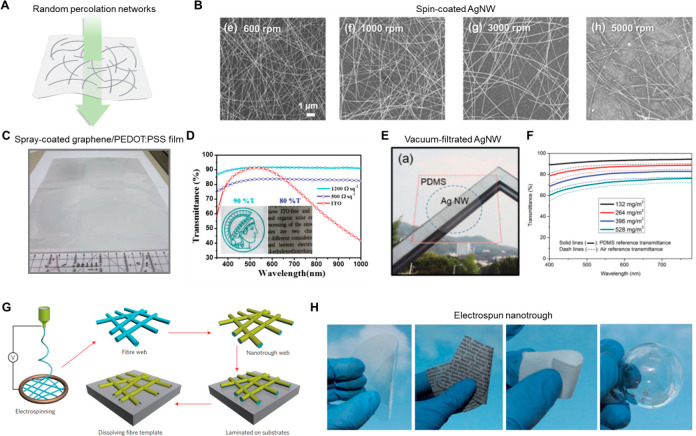
Figure 11.
Random percolation networks. (A) Schematic illustration of transparent electronics enabled by random percolation networks of electronic materials. (B) SEM image of spin-coated AgNW random percolation networks depending on spin rates. Reproduced with permission from ref (493). Copyright 2013 Wiley-VCH. (C) Optical image of a spray-coated large area of rGO sheet. (D) The transmittance of a large area of rGO with over 80% in the visible range. Reproduced with permission from ref (286). Copyright 2014 Wiley-VCH. (E) Optical image of vacuum filtration transferred transparent AgNW conductor on PDMS substrate. (F) The transmittance of AgNW transparent conductor by varying the density of random percolation networks. Reproduced with permission from ref (153). Copyright 2015 Wiley-VCH. (G) Schematic illustration of electrospinning-based random percolation networks transparent conductor. (H) Optical images of electro-spun transparent conductors on various substrates. Reproduced with permission from ref (499). Copyright 2013 Springer Nature.

