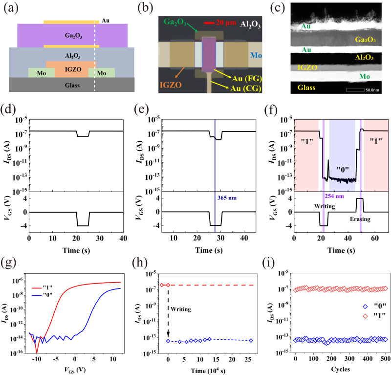
Fig. 3. The structure and performance of the final PSD-based optoelectronic memory device.
a Schematic diagram of the device. b Top view of the magnified optical micrograph of the fabricated device. c TEM cross-sectional image corresponding to the position of the white dashed line in (a). d The writing result by VGS = −4 V pulse. e The writing result by a combination of VGS = −4 V pulse and a 365 nm of 160 µW cm−2 optical pulse. f The single write/erase process and corresponding results. (optical pulse: 254 nm, 160 µW cm−2, 1 s; VGS pulse: −4V / 4 V). g Transfer characteristic curves in states “0” and “1”. h Retention test for up to 72 h. (optical pulse: 254 nm, 160 µW cm−2, 1 s; VGS pulse: −4 V). i Fatigue test result for 500 cycles. (optical pulse: 254 nm, 160 µW cm−2, 1 s; VGS pulse: −4 V/4 V). g–i Blue represents “0”, and red represents “1”.

