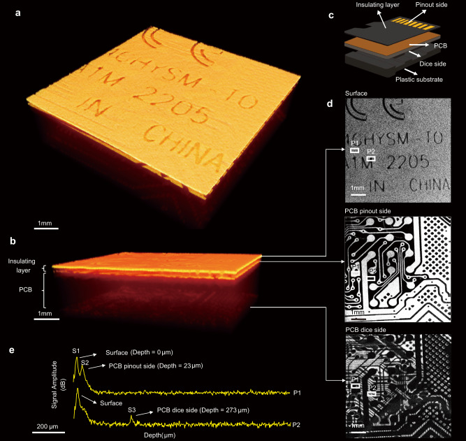
Fig. 2. Tomographic analysis of the multilayer structure of a micro-SD Card.
a 3D OCT image of the multilayer structure in a top-to-bottom view. b 3D OCT image of the multilayer structure in a cross-sectional view. c Diagram of the multilayer structure of a micro-SD card, including an insulating layer, PCB and plastic substrate. d En face OCT images at three different depths: Top—surface (depth = 0 μm), Middle —PCB pinout side (depth = 23 μm), Bottom—PCB dice side (depth = 273 μm). e Averaged A-scans at two different positions, P1 and P2, marked as white rectangles in (d). S1 corresponds to the surface of the micro-SD card. S2 represents the boundary between the insulating layer and the PCB. The distance between S1 and S2 represents the thickness of the insulating layer, estimated to be ~23 μm. S3 indicates the reflection of light from the copper conductive layer on the dice side of the PCB, suggesting the thickness of the PCB to be ~250 μm.

