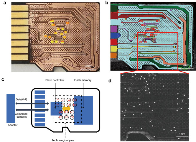
Fig. 4. Identification of pins and vias.
a The microscopic image of the exposed PCB on the pinout side obtained after removing the insulating layer. b The en face image of the PCB on the pinout side obtained by robotic-OCT imaging before the removal process. c The scheme of data extraction from flash memory of a micro-SD card. d The distribution of vias appearing as white spots in the en face image of the region indicated by the red rectangle in (b), at a depth of ~66 μm below the surface of the insulating layer. D0, D1, D2, D3, D4, D5, D6, and D7 represent the data I/O signal pins, while address latch enable (ALE), chip enable (CE), command latch enable (CLE), read enable (RE) and write enable (WE) denote the command signal pins.

