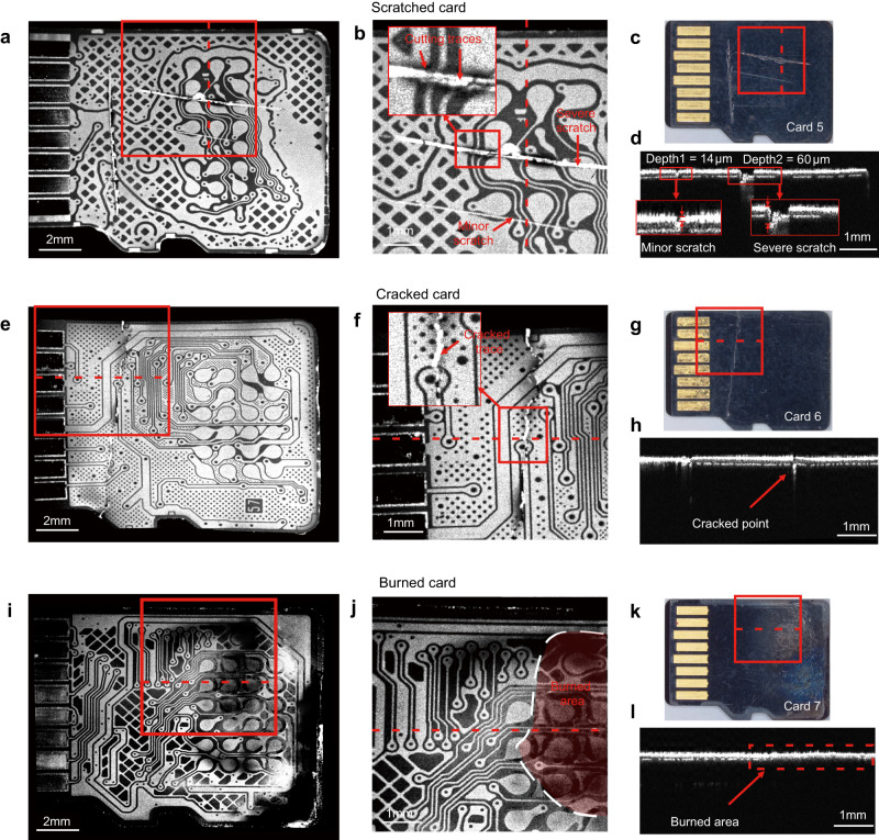
Fig. 5. OCT Images of scratched (Card 5), cracked (Card 6), and burned (Card 7) micro-SD Cards.
a En face OCT images of the PCB traces on the pinout side of Card 5. b Enlarged en face OCT images of the area indicated by the red boxes in (a, c), clearly showing minor scratch, severe scratch, and cutting traces. c Microscopic images of Card 5. d Corresponding B-scan to the red dashed lines in (a–c), indicating the depths of the minor and severe scratches to be approximately 14 μm and 60 μm, respectively. e En face OCT images of the PCB traces on the pinout side of Card 6. f Enlarged en face OCT images of areas indicated by the red boxes in (e, g), clearly showing the cracked trace. g Microscopic images of Card 6. h Corresponding B-scan to the red dashed lines in (e–g), indicating the position of the cracked point. i En face OCT images of the PCB traces on the pinout side of Card 7. j Enlarged en face OCT images of areas indicated by the red boxes in (i, k); the red area indicates the burned area, and the white dashed line represents the boundary of the burned area. k Microscopic images of Card 7. l Corresponding B-scan to the red dashed lines in (i–k). The area enclosed by the red dashed line indicates the burned area, which has a different cross-sectional structure compared to the surrounding unburned area.

