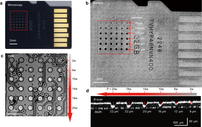
Fig. 7. Evaluation of different power levels on the laser ablation process.
a Microscopic image showing a micro-SD card ablated with six different power levels. b En face OCT image of the ablated card surface; the diameters of the ablation holes for six power levels (2 W, 6 W, 10 W, 14 W, 18 W, and 20 W) are measured to be 75 μm, 140 μm, 170 μm, 220 μm, 230 μm, and 260 μm, respectively. c En face OCT image of the ablated card at a depth of ~20 μm (pinout side of the PCB), demonstrating the precise positioning and different sizes of the ablation holes at six power levels (2 W, 6 W, 10 W, 14 W, 18 W, and 20 W). d B-scan at the red dashed lines in (b), indicating the maximum depths of the ablation holes at six power levels (2 W, 6 W, 10 W, 14 W, 18 W, and 20 W) to be 9 μm, 12 μm, 18 μm, 20 μm, 22 μm, and 22 μm, respectively.

