
Figure 3.
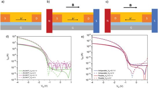
a) Geometry of a BGBC device with Au electrodes, b) representation of a BC device in a parallel magnetic field, and c) in an antiparallel magnetic field. Gate contact (G) is depicted in gray, the dielectric in light blue, source (S) and drain (D) gold contacts in orange and the semiconductor in yellow. The direction of the magnetic field (B) and of the hole current (h+) are depicted with black arrows. d) Transfer curves of (R)‐DNTT (green) and (S)‐DNTT (pink) best performing OFETs fabricated with BGBC geometry at a substrate temperature of 40 °C. e) Transfer curves of (S)‐DNTT BC OFETs placed in a parallel (red) and antiparallel (blue) magnetic field.