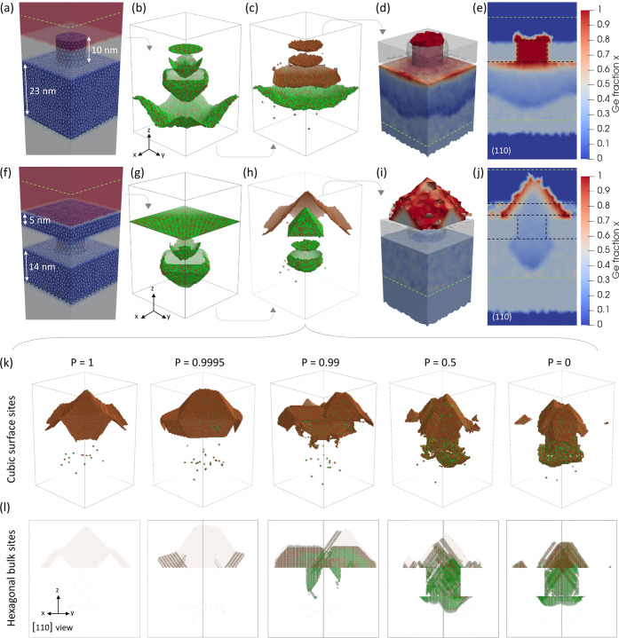
Figure 6.
(a–e) Pulsed-LA simulation (308 nm, 22 ns, 0.95 J cm–2) of 30 nm strained Si0.6Ge0.4 with 9 nm large and 10 nm high Si0.6Ge0.4 NWs on top, embedded in nonmelting SiO2. (a) Input FEM periodic mesh. KMCsL-coupled SiGe regions are shown in blue, air in red, and SiO2 and non-KMCsL-coupled regions in gray. The KMCsL cell extension along z is indicated with dashed green lines. (b) Overlapped selected snapshots of the liquid–solid interface in the KMCsL box at various instants during melting and (c) solidification. Green (brown) spheres indicate Si (Ge) atoms. (d) 3D view and (e) (1 1 0) cut-plane of the final Ge distribution in the FEM mesh. Regions outside the KMCsL cell (below the green dashed line) appear uniformly colored because no KMCsL mapping occurs therein. The initial surface morphology is indicated by dashed black lines. (f–j) Simulation at a 1.2 J cm–2 energy density for the same system as above, including a 5 nm thick Si0.6Ge0.4 capping layer. (k) Cubic undercoordinated sites in the KMCsL box at the end of the simulations performed at the same conditions as (f–j) but with different polymorphic solidification probabilities P. (l) Hexagonally stacked sites (regardless of coordination) from the simulations in panel (k), viewed along the [1 1 0] direction. Cubic sites from panel (k) are redrawn in semitransparency.

