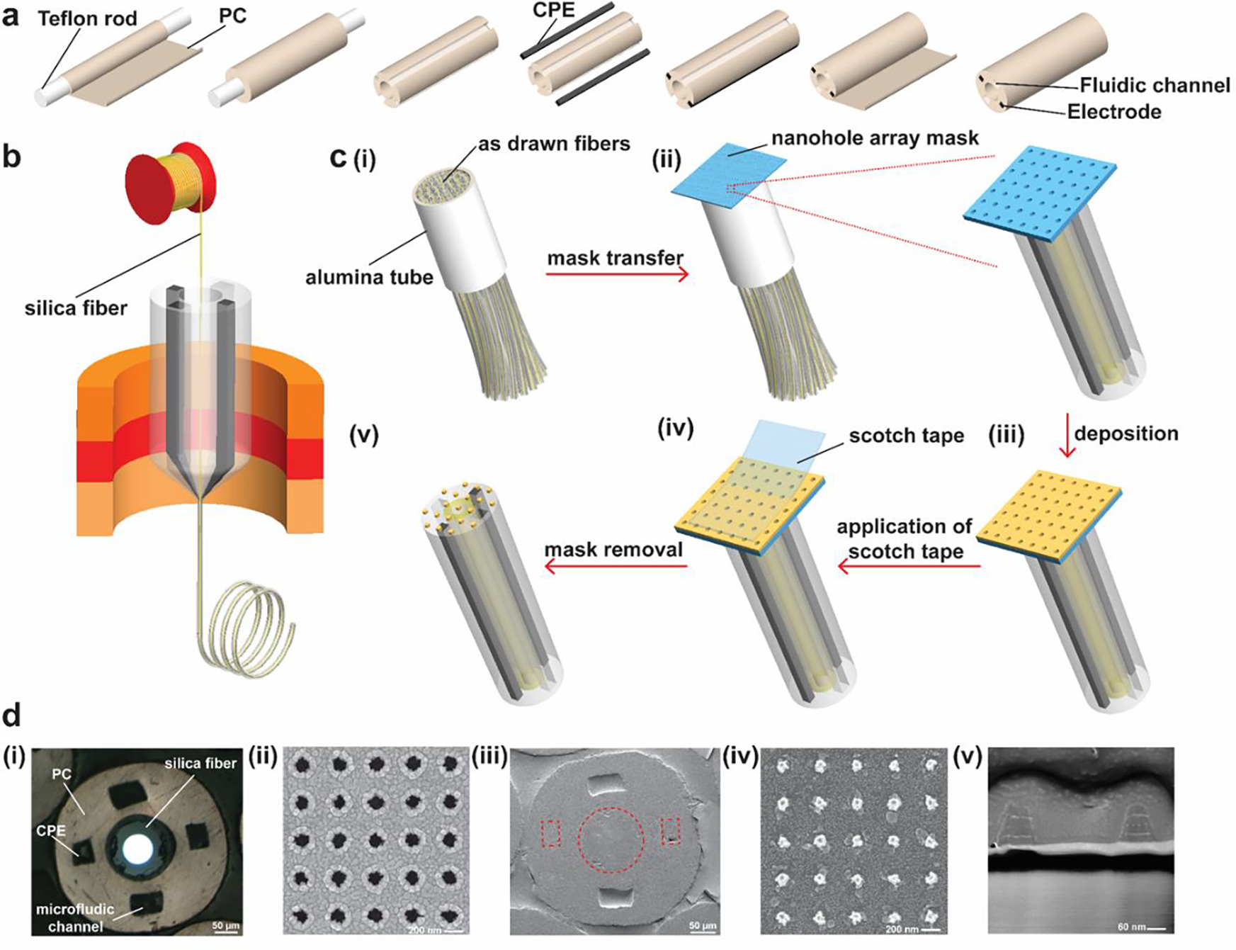
Figure 1.

Fabrication of nano-optoelectrodes on multifunctional fiber tips. (a) A schematic showing the fabrication process of the preform with two electrodes, two fluidic channels, and a hollow core. (b) An illustration of the fiber drawing process. The silica fiber was inserted into the center hole and converged with the polymer material during the thermal drawing process. (c) Schematic illustration of the process of integrating the nano-optoelectrodes on the fiber tips: (i) As-drawn fibers were cut, bundled, and inserted into an alumina tube; (ii) After the fixation and polishing process, a nanohole array mask was transferred to the top surface of the bundle; (iii) Following the mask transfer, layers of Ti, Au, and Ag were deposited onto the polymer fiber bundle tip via e-beam evaporation; (iv) The nanohole array mask was peeled off using scotch tape, leaving behind the periodic nanostructures as shown in (v). (d) Optical and SEM images of the multifunctional fiber, nanohole array mask, and the nano-optoelectrodes: (i) Optical image of the as-drawn multifunctional fiber in the bundle after polishing; (ii) SEM image of the nanohole array mask; (iii) SEM image of the fiber tip with periodic nano-optoelectrodes deposited; (iv) A zoomed-in SEM image showing the nano-optoelectrodes on the silica fiber; (v) A cross-sectional SEM image of the nano-optoelectrodes.
