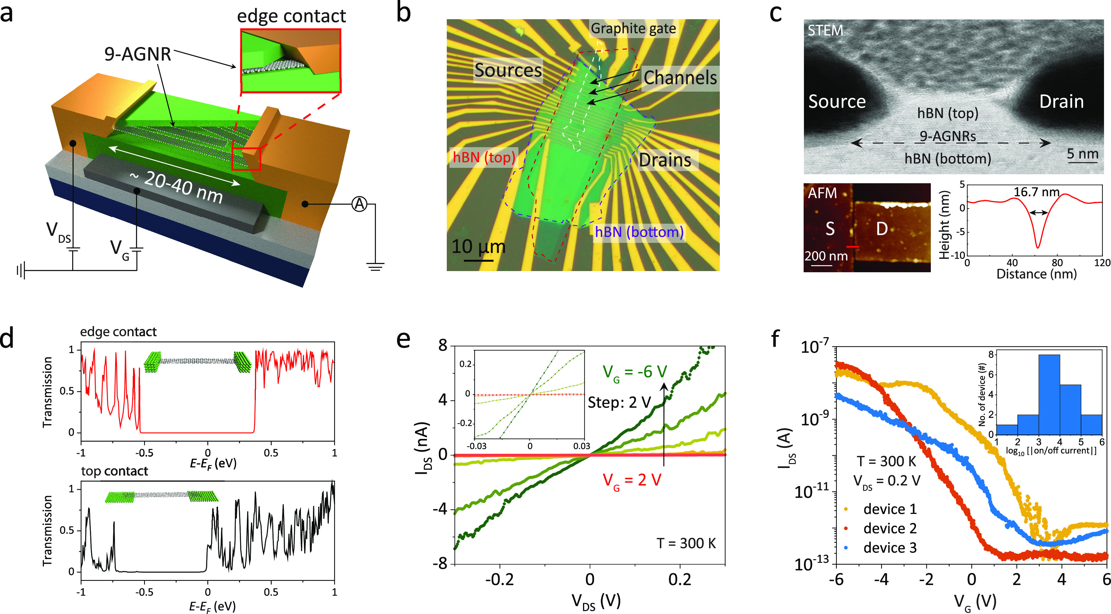
Figure 1.

Device geometry and characterization. (a) Structure schematic of the 9-AGNRs SCFETs, including the measurement circuit. The film of 9-AGNRs is encapsulated between the top and bottom h-BN (light green), placed on a graphite gate (dark gray), and contacted by edge contacts (yellow). We measure the source–drain current (IDS) upon the application of source–drain bias (VDS) and gate voltage (VG). The top right inset shows a zoom-in configuration of the edge contact. (b) Optical micrograph of the measured device. The edges of the graphite gate (white), the bottom (purple) h-BN, and the top (red) h-BN are indicated by dashed colored lines. Source and drain contacts are labeled S and D, respectively. Their separation, labeled as channel, is below the resolution limit (∼20–40 nm). The channel width is ∼500 nm. (c) Top: STEM image showing a device cross-section. Arrows highlight the positions of the 9-AGNRs layer. Bottom left: AFM image of the channel region between the S and D contacts. Bottom right: line scan indicating the S and D contact separation (red line in the bottom left panel). (d) Computed transmission curves of edge contacts versus top contacts for chromium electrodes. The schematics illustrate the two contacting geometries: edge-contact (top) and top-contact geometry (bottom). (e) IDS–VDS characteristics of representative SCFET devices at different VG at 300 K. Inset: zoom-in of the low-bias range. (f) IDS vs VG curves at fixed VDS = 0.2 V for 3 representative SCFET devices at 300 K. Inset: histogram of the on/off ratio for all measured SCFETs.
