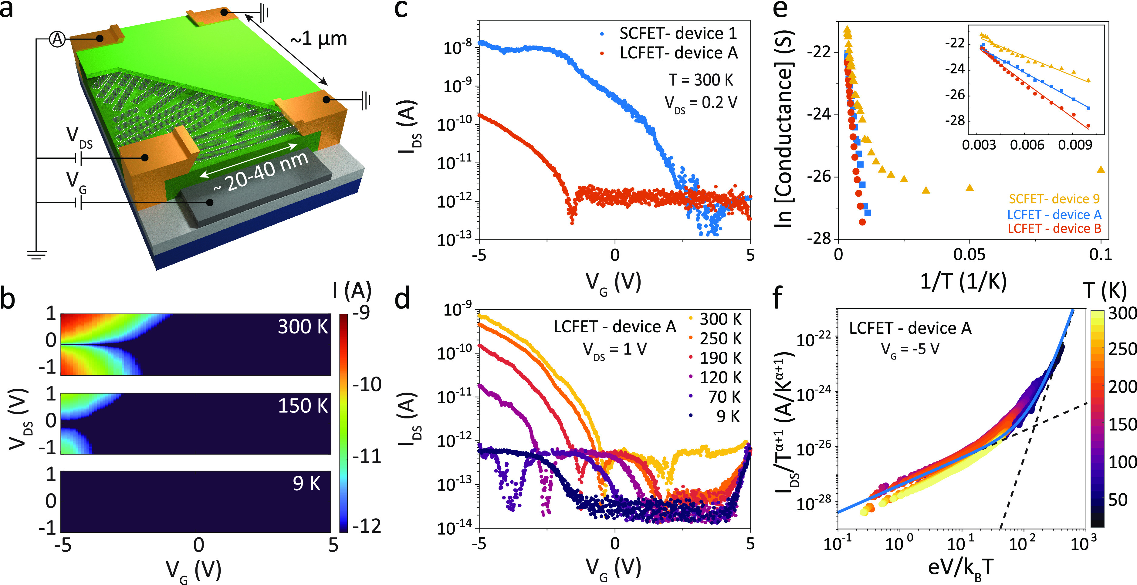
Figure 3.

Charge transport in GNR networks. (a) Schematic illustration of long-channel FETs (LCFETs) with the measurement circuit. The film of 9-AGNRs is encapsulated between h-BN (light green), placed on a graphite gate (dark gray), and contacted from the side by edge contacts (yellow) separated by a larger distance than the average 9-AGNR length, in the range of μm. We measured the IDS upon application of VDS and VG. (b) Maps of IDS as a function of VDS and VG recorded on device A at various temperatures (only 9, 150, and 300 K, shown here; see more details in Supporting Information Figure S16). (c) Transport characteristics of SCFET device 1 and LCFET device A as a function of VG, recorded at 300 K (VDS = 0.2 V). (d) Transport characteristics of device A at fixed VDS = 1 V as a function of VG, recorded at various temperatures. (e) Arrhenius plot of the conductance recorded from three different devices at VDS = 0.4 V and VG = −5 V as a function of 1/T. The inset is linear fittings within 300 to 100 K for these three different devices. (f) The temperature-dependent current–voltage characteristics at VG = −5 V as scaled current I/Tα+1 versus scaled bias voltage eV/kBT.
