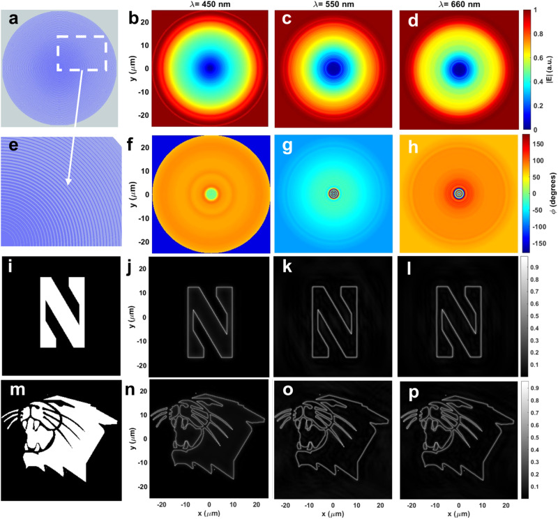
Fig. 2. 3D device simulations in visible wavelengths.
a The designed complete layout and (e) a closer image of the 3D metasurface: co-centric Aluminum rings of 70 nm fixed height and varying width on top of a SiO2 substrate. b–d The simulated amplitude and (f–h) phase maps of the transmitted electric field at 450,550, and 660 nm wavelengths using the hypothetical device shown in (a). i The letter “N” of Northwestern University logo and (m) the Northwestern Wildcats logo as the input fields. j–l, n–p The calculated output fields of the 4f system with the metasurface.

