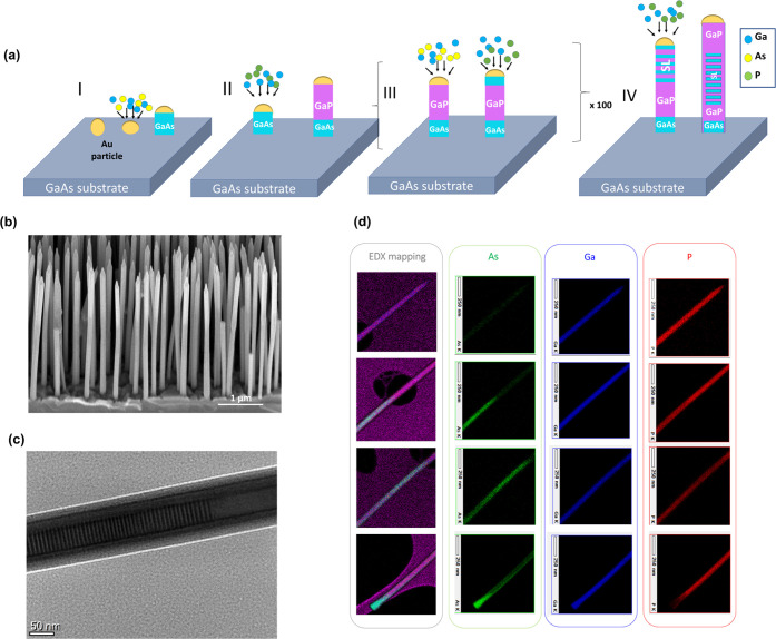
Figure 1.
GaAs/GaP superlattice nanowires. (a) Schematic illustration of the four-step growth process of a typical GaAs/GaP SL NW using chemical beam epitaxy; (b) SEM image of as-grown free-standing GaAs/GaP SL NWs grown on GaAs substrate; (c) TEM image of a typical SL NW of a nominal period 10 nm dispersed in a holey carbon grid investigated in this work; (d) the EDX mapping of SL NW with 4.8 nm period in false colors shows the distribution of elements along the length of the wire showing the presence of the GaAs/GaP SL segment. The elemental maps of one NW are represented as follows: green for As, blue for Ga, and red for P.

