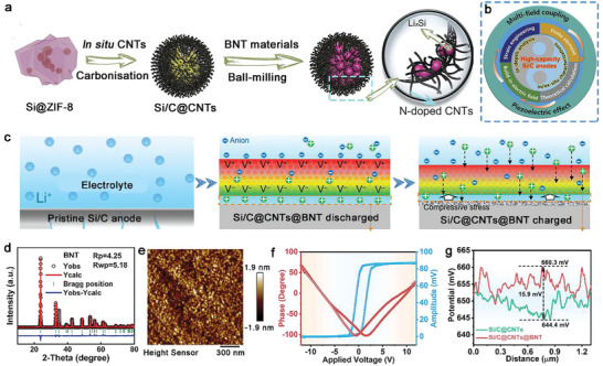
Figure 1.

Design and characterization of poled BNT‐coated Si/C. Schematic illustration of deposition morphology, electric field, and ion flux distribution on a) bare Si and b) poled BTO‐coated Si. c) Schematic illustration of the regulation effect of piezoelectric BNT layer on Li+ transportation at Si/C interfacial. d) XRD pattern with FullProf refinement data for the as‐prepared pure BNT. The corresponding piezoresponse force microscopy (PFM) e) phase and f) amplitude hysteresis loops for BNT particles. g) Corresponding surface charge difference profile of Si/C@CNTs@BNT and Si/C@CNTs.
