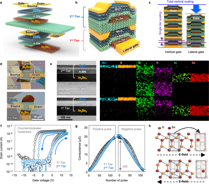
Fig. 1. The schematic structure and electrical characteristics of the LG-FeFET.
a The configuration of the layers and b the integrated structure of a two-tier LG-FeFET device. c A conceptual comparison between the LG-FeFET and a conventional vertical FeFET structure. d Optical microscopy images of the devices on the first and second tiers. The source and drain electrodes of the second device are aligned with those of the first device. e The transmission electron microscopy (TEM) image and the corresponding energy-dispersive X-ray spectroscopy in scanning transmission electron microscopy (STEM-EDS) images of the cross-section of the two-tier device. f Double-sweep Id–Vg transfer curves for both first and second tiers. The arrows in the loop indicate the sweep directions of the gate voltage. g The change of conductance for the incremental step positive (from −1.8 V to 0.5 V) and negative gate pulses (from −1.9 V to −4 V) with an identical read voltage (−1.8 V). h The atomic structures of α-In2Se3 (Se-In-Se-In-Se) under the external electric field.

