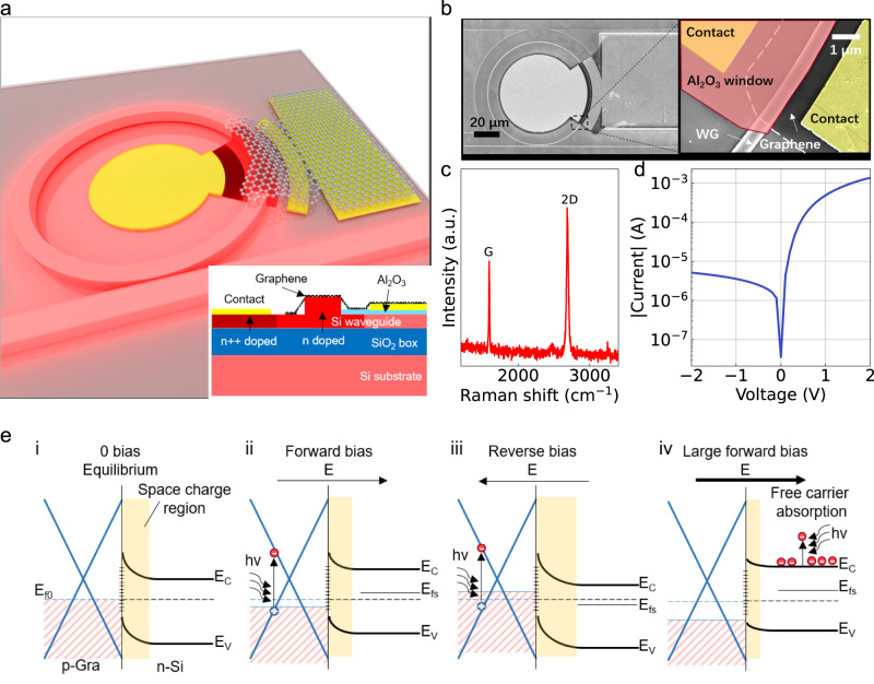
Fig. 2. Schematic illustration, properties and operation principle of the graphene/silicon heterojunction.
a Three-dimensional schematic of the graphene/silicon heterojunction device. Inset is the cross-section of the heterojunction structure before photoresist coating. b SEM image of the top-view of the heterostructure. c Raman spectrum of the graphene. d Current-voltage curve of the heterojunction indicating that the device is a heterojunction. e Energy-band diagrams of Gra/Si heterostructure. i thermal equilibrium and dark cases at 0 bias. Ef0, EC and EV are the initial Fermi level of the heterojunction, conduction-band bottom and valence-band top of silicon, respectively. ii: band structure under forward bias condition. Efs is Fermi level the silicon. iii: band structure at reverse bias. iv: band structure at large forward bias where the free carrier absorption dominates. The space charge regions are plotted in wheat-colored blocks and the surface states are marked (+) at the Gra/Si interface.

